
PCB Manufacturing Capabilities
The process envelope in full — 0.075 mm trace and space, 32 layers, 12 oz copper, ±5% impedance, 28 GHz RF. Published as limits, with the conditions attached to each one.
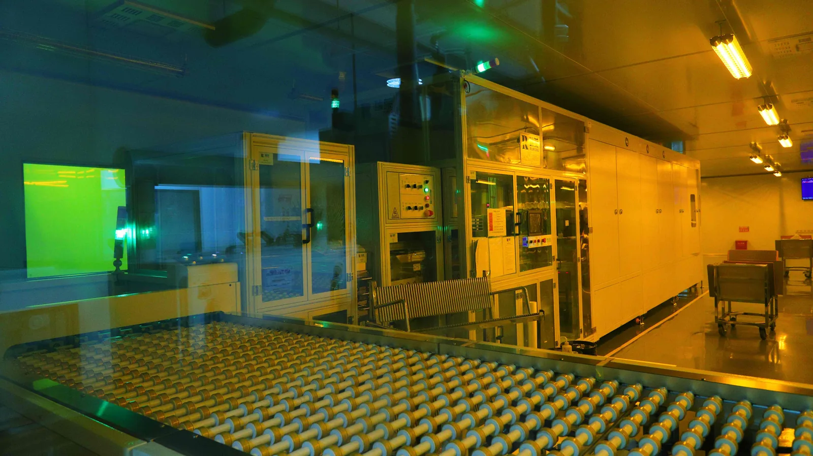
The limits are the product.
This page is the process envelope, written down. Every figure here is the same figure our CAM team quotes against and the same figure the board-type pages cite — one table, one source, changed when the floor changes rather than when a brochure is due.
Most suppliers answer a capability question with an adjective. Ours is answered with a limit and the condition attached to it: what runs in standard production, what is available on request, and what we will decline rather than attempt. If a number is not on this page, we do not build it yet.
What the floor holds, line by line.
A · Board structure and layer count
| Parameter | Capability |
|---|---|
| Layer count | 2–32 layers standard; 50+ on inquiry (sequential lamination) |
| Max panel size | 600 × 900 mm |
| Board thickness | 0.4–6.0 mm (standard FR-4) |
| Layer registration | ±50 µm |
B · Circuit and drilling
| Parameter | Capability |
|---|---|
| Min trace / space | 0.075 mm / 0.075 mm |
| Mechanical drill | from 0.15 mm |
| Laser drill | from 0.1 mm |
| Aspect ratio | 12:1 standard; 20:1 on inquiry |
| Back-drill depth control | ±0.05 mm |
C · Copper and impedance
| Parameter | Capability |
|---|---|
| Inner copper | 0.5–4 oz |
| Outer copper | 0.5–6 oz standard; 12 oz on inquiry |
| Impedance tolerance | ±5% standard; ±3% on request; TDR coupon per lot |
| RF verification | to 28 GHz on coupon |
D · Test, build limits and derating
| Parameter | Capability |
|---|---|
| Electrical test | 100% — flying probe on prototypes, fixture on volume |
| HDI lamination cycles | up to 4 |
| Rigid-flex layer ceiling | up to 16 layers including polyimide |
| Metal-core copper layers | 1–2 |
| Copper weight conversion | 1 oz ≈ 35 µm; 12 oz ≈ 420 µm |
UL 94 V-0 · IPC-6012 / IPC-A-600 · IPC Class 2 standard, Class 3 on request · Laminate families, finishes and the test sequence: see the detail pages below.
The six places orders get hard.
Any-layer HDI
Microvias stacked pad-on-pad or staggered through every layer, with the drill programme qualified on your laminate rather than on a sample stack.
Controlled impedance and back drilling
Impedance modelled before lamination and measured on a coupon after it. Back-drilled vias get a depth window per span and a cross-section to prove it.
Heavy copper and thermal design
Etch compensation, prepreg fill and thermal-via placement are set per copper weight, because a 6 oz trace etches nothing like a 1 oz one.
Ceramic and metal-core substrates
Heat leaves through the substrate instead of the copper. Dielectric thickness and base metal are chosen against junction temperature, not against a catalogue page.
Rigid-flex and sequential lamination
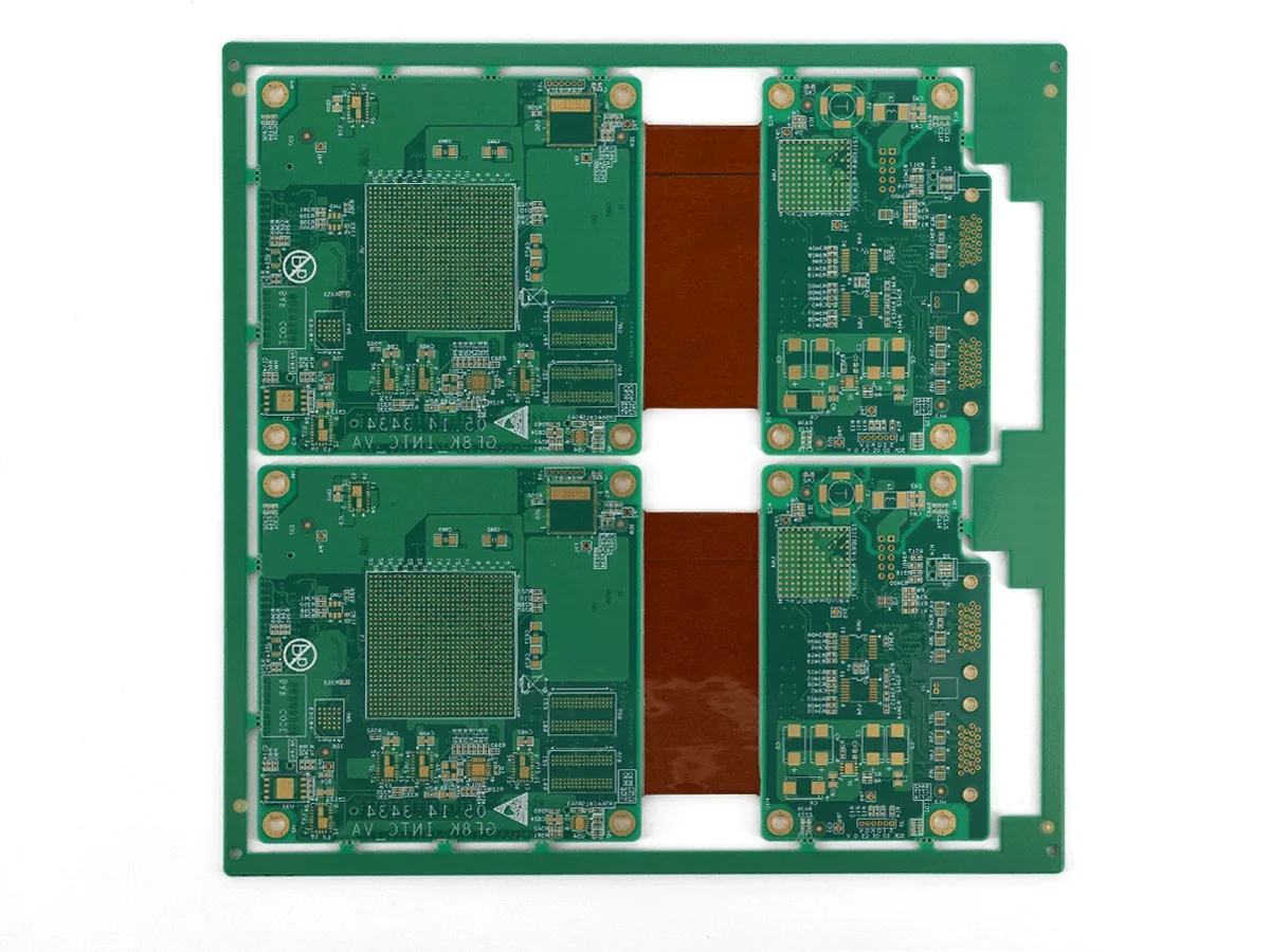
Rigid stack-up, bend area and stiffener are reviewed as one system, because failures collect at the transition rather than in either section.
High-layer-count and registration
Past twenty layers the press curve decides yield. Ramp rate and pressure are set per prepreg combination, with inner-layer AOI gating every cycle.
Not sure which limit your design actually hits?
Send the files — the answer comes back from a CAM engineer, with the constraint named.
Where each section goes deeper.
Surface Finish
ENIG, HASL-LF, OSP, immersion silver, immersion tin and hard gold — with the four questions that decide between them.
Materials
Five laminate families, the grades we hold in stock, and the Dk / Df figures the signal actually sees.
Testing and Inspection
Eight gates from incoming material to final release, with the Class 3 flow quoted per order.
PTFE
Low-Dk substrates down to 2.20, and the point where an all-PTFE stack stops making sense.
High-Tg FR4
Tg 170–180°C laminates for repeated reflow and thermal cycling, including halogen-free grades.
Eight gates, and nothing ships without passing all of them.
Incoming material
Laminate and copper checked against the lot certificate before release to imaging.
Inner-layer AOI
Opens, shorts and dimension errors caught while they can still be reworked.
Lamination
Press curve per prepreg combination; registration verified after each cycle.
Drill and plating
Hole position and wall thickness sampled per panel, not per lot.
Electrical test
100% — flying probe on prototypes, fixture on volume builds.
TDR correlation
Coupon on every production panel; measured values ship with the CoC.
Cross-section
Couponed builds cut and read for dielectric, plating and residual stub.
Final release
Documentation, CoC and IPC class stated per order before the carton closes.
The standards our systems are audited against.

ISO 9001:2015

IPC-A-610

IATF 16949:2016

ISO 13485

ISO 14001:2015

UL

RoHS

REACH
Badges show the standards our quality system is audited against. Certificate numbers and current validity are supplied on request, per certification.
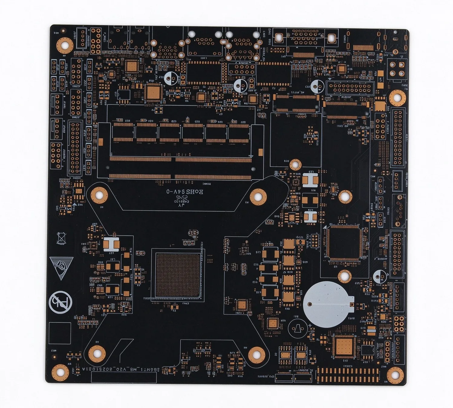
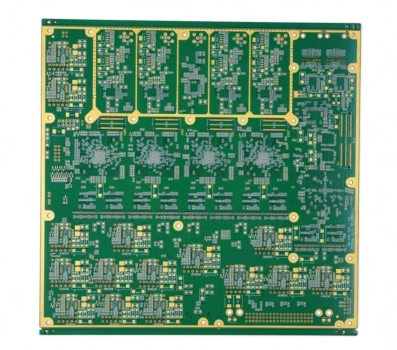
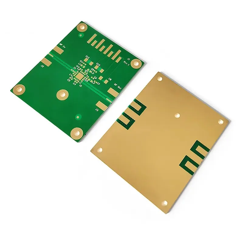
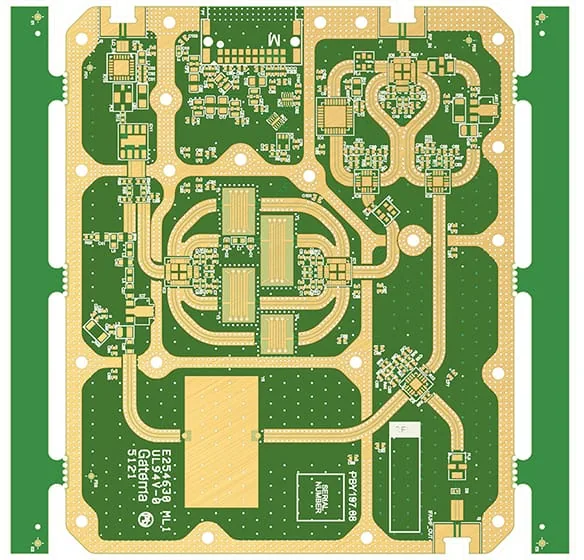
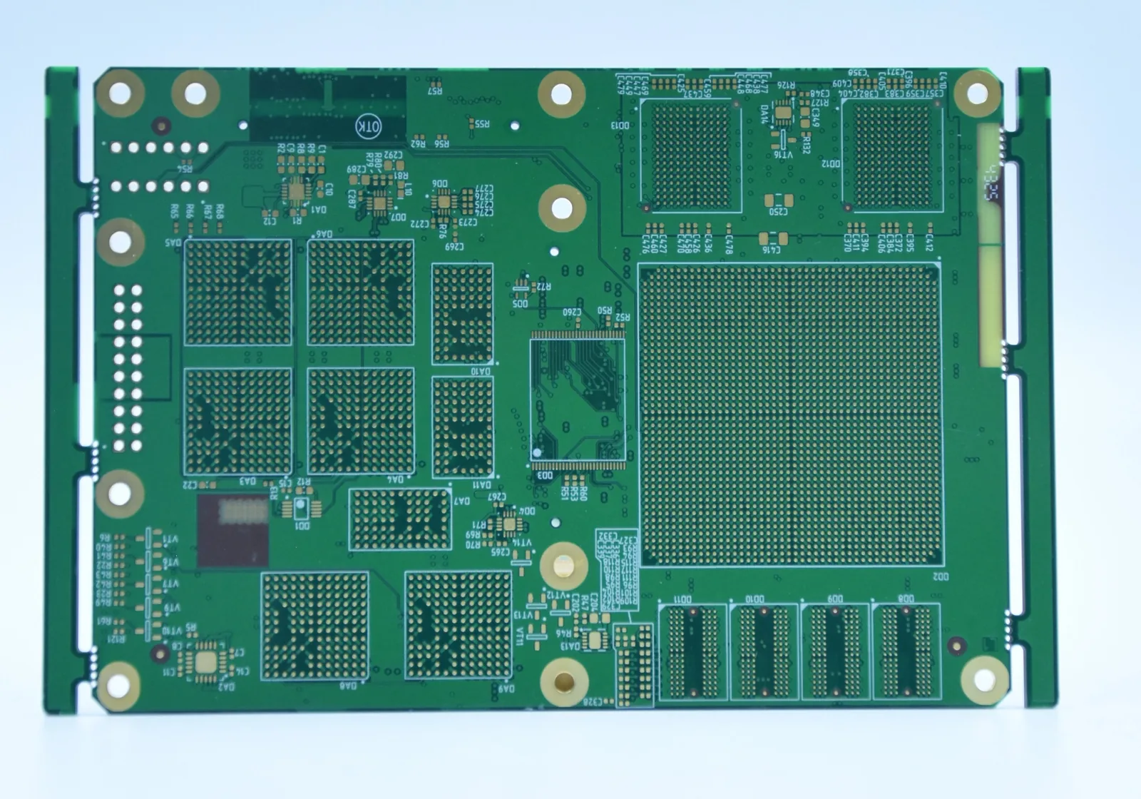
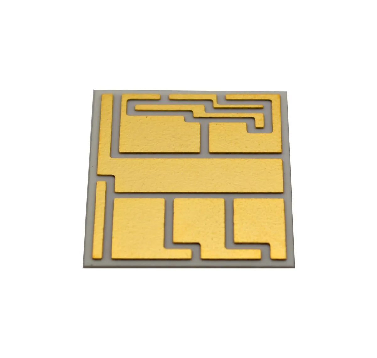
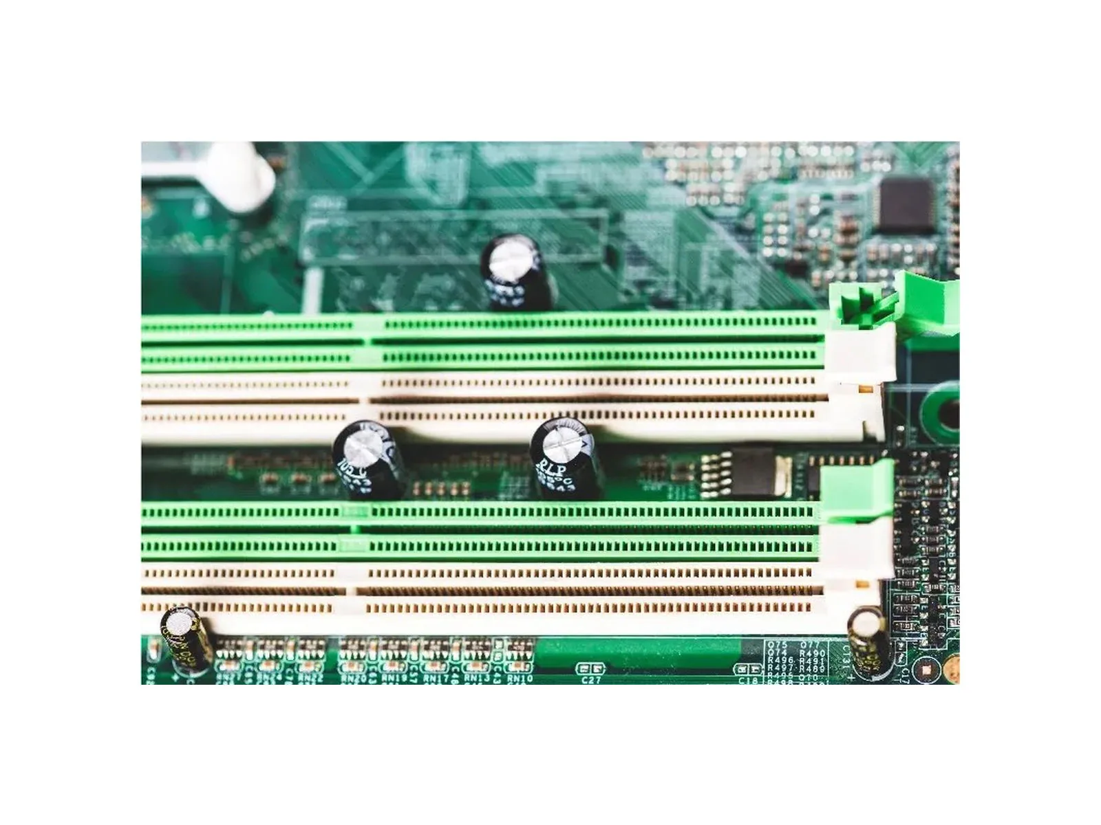
What those limits look like when they ship.
Questions about the limits themselves.
What is the largest board you can build?
600 × 900 mm panels, with layer count to 32 in standard production and 50+ on inquiry. Thickness runs 0.4–6.0 mm on FR-4; metal-core builds run 0.8–3.2 mm.
Which impedance tolerance should I specify?
±5% is the standard window and the one most designs actually need. ±3% is available on request — it changes the stack-up and the price, so it is worth deciding before layout rather than after.
Are the numbers on this page current?
They are the figures our CAM team quotes against. When the floor changes a limit this page changes with it, and the board-type pages follow the same table.
Do you publish certificate numbers?
The badges above show the standards our quality system is audited against. Numbers and validity dates are supplied per certification on request.
How fast is a quotation?
Quote in 24 hours for most orders. If a design needs a stack-up discussion first, the engineering query comes back inside that window instead of a price.
Need a limit confirmed before you commit to a design?
Ask before layout, not after. Quote in 24 hours.