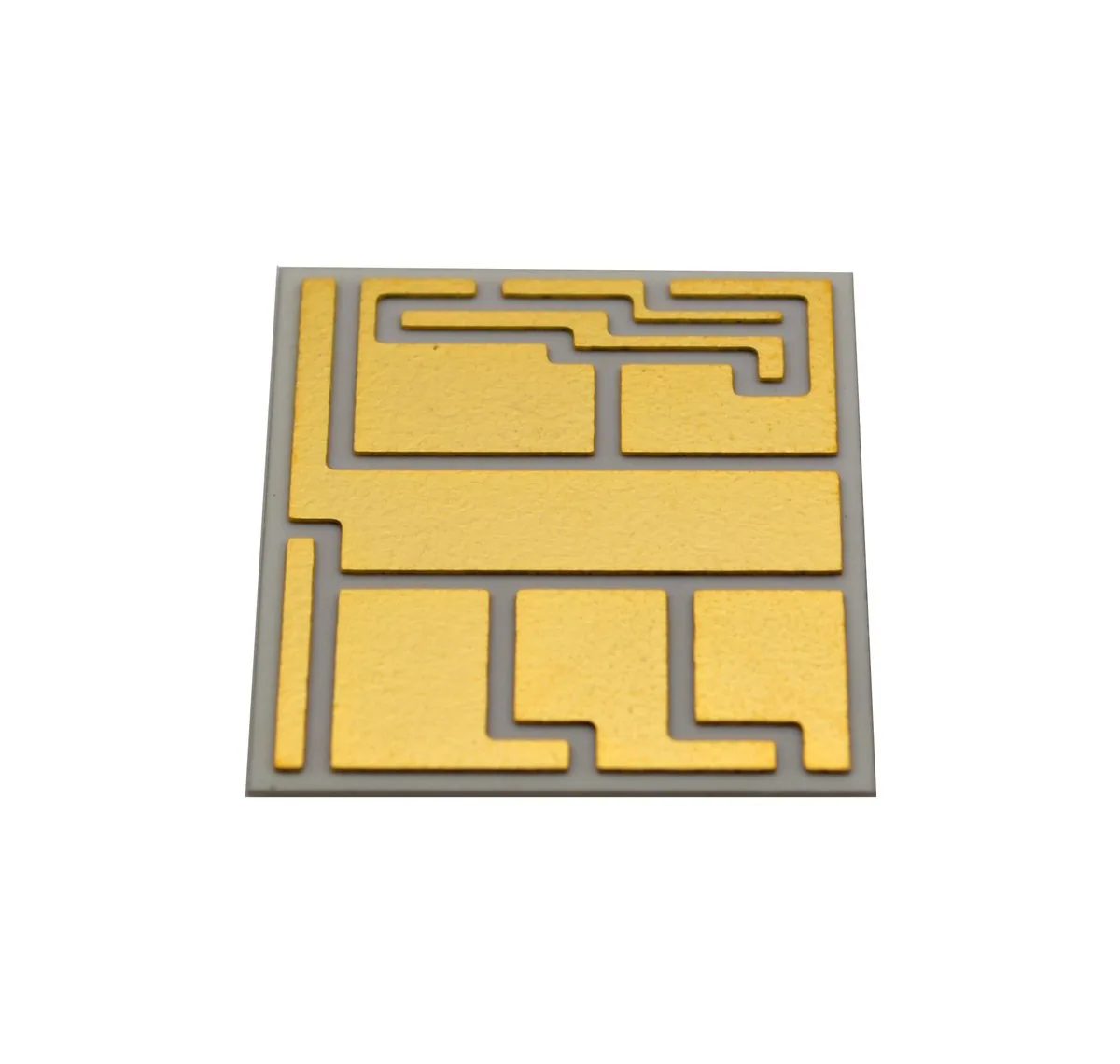
Ceramic vs FR-4: When the Substrate Becomes the Heat Sink
Alumina at 20–24 W/m·K and AlN at 170 against 0.2–0.3 for FR-4, plus the crossover arithmetic that decides which one ships.
Read article

Al₂O₃ at roughly 24 W/m·K and AlN at roughly 170 W/m·K — a substrate chosen for the thermal path first, with CTE close enough to silicon and GaN that the solder joint stops being the weak link.
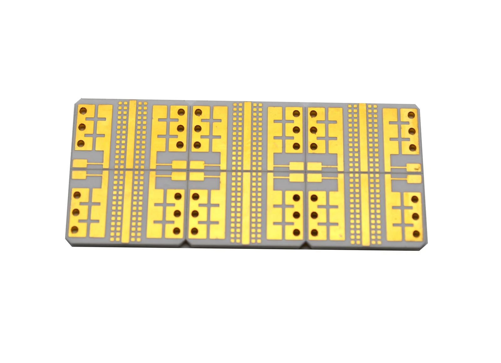
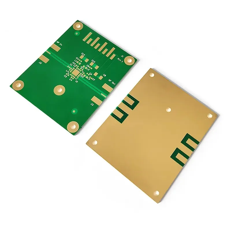
A ceramic PCB uses an aluminium oxide or aluminium nitride substrate in place of glass-epoxy laminate. The substrate is both the dielectric and the structural body: Al₂O₃ conducts around 24 W/m·K, AlN around 170 W/m·K, against roughly 0.3 W/m·K for FR-4. Both are electrical insulators, both survive temperatures that would char laminate, and both expand at 3–6 ppm/°C — close to silicon and GaN, so die attach and solder joints see far less strain across a thermal cycle.
Many fabricators list ceramic as a material option: you select it, the board runs on the same flow as FR-4, and the thermal path becomes your problem at assembly. We work from the other end — where the heat is generated, where it has to go, and which substrate and copper geometry get it there.
That means an engineering review before panelisation: AlN or Al₂O₃ by power density and budget, metallisation method (direct-bonded copper, active metal brazing or thick film), copper thickness and pattern, and a plating stack that suits your die-attach or soldering process. 80 CAM engineers review 6,000+ designs a month, and the first engineering response — substrate, metallisation, plating — usually comes back within 24 hours.
AlN versus Al₂O₃ is a thermal and cost decision, not a preference. Substrate is matched to power density first; then the copper bond — DBC, AMB or thick film — and its thickness are specified, because the metallisation is part of the heat path rather than a coating on top of it.
Ceramic is not routed, it is scribed and separated. Laser parameters follow substrate type and thickness so the kerf stays clean, edges do not chip, and no micro-crack is seeded for thermal cycling to open later. Outline and hole positions hold ±50 µm registration.
Copper on ceramic needs a barrier before it ever meets solder. ENIG or immersion silver is selected against the assembly route — die attach, wire bonding or reflow — with plating thickness controlled so the surface stays coplanar and keeps its shelf life.
Every ceramic design carries a CTE mismatch risk at the copper-to-substrate interface. Thermal shock and cycling, peel strength, solderability and cross-sections are used to prove the interface survives, not just that the board measures correctly at room temperature.
| Parameter | Capability |
|---|---|
| Al₂O₃ substrate | 96% alumina, ~24 W/m·K — the cost-efficient choice for most power and LED builds |
| AlN substrate | Aluminium nitride, ~170 W/m·K — for high power density and RF where heat cannot be spread |
| CTE | 3–6 ppm/°C, substrate-dependent; matched to silicon and GaN |
| Board thickness / panel | 0.4–6.0 mm overall board thickness; panel up to 600 × 900 mm |
| Metallization | Direct-bonded copper (DBC), active metal brazing (AMB) or thick film; copper 0.5–6 oz outer |
| Min trace / space | 0.075 mm / 0.075 mm; defined per copper weight on heavy builds |
| Layer count | 2–32 layers standard; 50+ on inquiry |
| Electrical test | 100% — flying probe or fixture, with thermal-cycling samples on request |
RoHS / REACH · IPC-6012 / IPC-A-600 · IPC Class 2 standard, Class 3 on request · Full matrix: see Capabilities.
Send the thermal map with the files — an engineer reads both, then answers.
AlN carriers and DBC substrates for RF amplifiers where heat density rules out laminate.
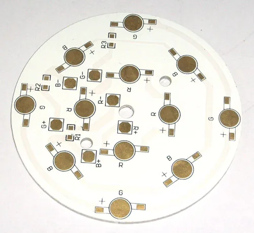
Alumina boards for LED arrays that must hold colour and life at high junction temperature.
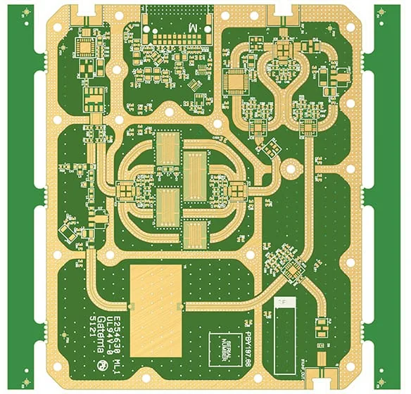
DBC and AMB substrates for IGBT and SiC modules with copper bonded on both faces.
Substrates that keep their electrical behaviour from cryogenic cold to engine-bay heat.
Alumina at 20–24 W/m·K and AlN at 170 against 0.2–0.3 for FR-4, plus the crossover arithmetic that decides which one ships.
Read article
At 3 oz the etchant travels sideways through 105 µm of copper, so the minimum space opens to 0.20 mm and the trace section becomes a trapezoid.
Read article
Two resin systems through one press cycle, a 190 °C compromise profile, and why desmear behaves differently on each plastic.
Read article
Go by power density and thermal resistance, not by price alone. Al₂O₃ at ~24 W/m·K covers most power and LED designs; AlN at ~170 W/m·K is for high power density and RF where heat cannot spread far. Send the thermal map during engineering query and we will compare both on your stack.
2 to 32 layers in standard production and 50+ on inquiry, with multilayer ceramic (LTCC) reviewed per design. Most power substrates are single- or double-sided metalised; multilayer is used when RF or control routing has to share the substrate.
Direct-bonded copper, active metal brazing or thick-film metallisation, finished with ENIG or immersion silver suited to die attach, wire bonding or reflow. Plating thickness and coplanarity are agreed at quotation, together with the finish on each side.
Gerber (RS-274X) or ODB++ with drill and outline files, the substrate callout (Al₂O₃ or AlN, thickness), copper thickness and the assembly method. Add the thermal requirement if you have one — a CAM engineer reviews the files, not a form.
Ceramic builds are quoted with lead time confirmed at quotation, because substrate availability and the metallisation route change the schedule. We put the date in writing and raise any change before it turns into a delay.
Send the files and the thermal requirement. Quote in 24 hours.