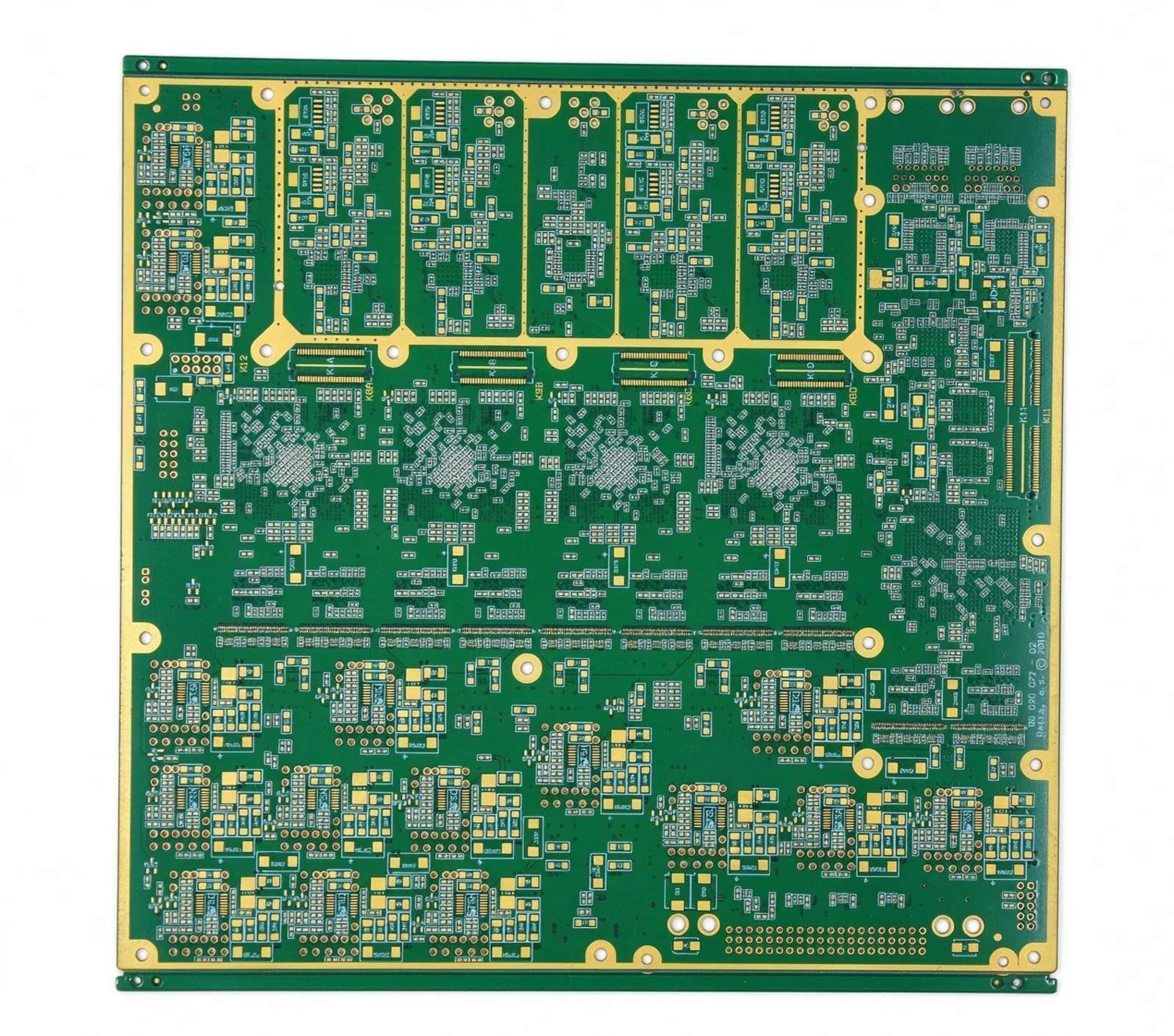
How to Design for HDI: Microvia Stacking and Any-Layer
What each BGA pitch band demands in via type, line width and stack-up, from 1.0 mm down to 0.35 mm.
Read article

Any-layer microvias, 0.1 mm laser drills and up to four lamination cycles — with the engineering review finished before the first panel is imaged, not after.
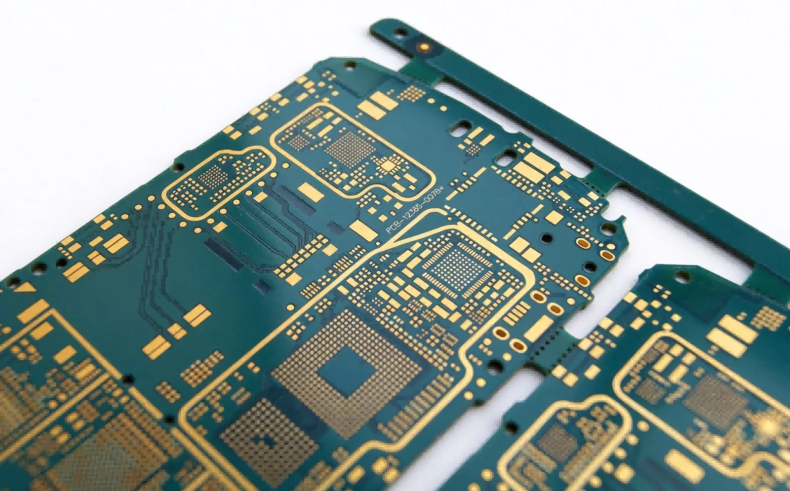
HDI PCB replaces part of the mechanical drill programme with laser-drilled microvias, finer conductors and sequential lamination. The payoff is routing density per square centimetre, shorter return paths and a workable escape for fine-pitch BGA — the combination that dense AI, RF and handheld hardware cannot be built without.
Many fabricators sell HDI as a feature list and hand the hard decisions back to the customer. We take the opposite position: an HDI stack-up is a set of coupled choices — via type, aspect ratio, lamination count, fill, impedance — and an error in any one of them surfaces only after lamination, when nothing can be reworked.
So the review happens before tooling. 80 CAM engineers work through more than 6,000 designs a month, confirming any-layer and stacked-via feasibility and returning engineering queries inside 24 hours. Fine-line imaging, 0.1 mm laser drilling, ±50 µm layer registration and 100% electrical test then carry the approved stack-up through to shipment.
Microvia quality is set by pulse energy, copper surface and dielectric, not by one recipe reused on every panel. The drill programme is qualified on your actual laminate and copper weight, so a 0.1 mm via lands centred on its target pad instead of skimming the edge.
Stacking a via onto the one below multiplies density, but each additional press carries its own registration budget. Cycle count is modelled against your escape requirement before the quote, keeping any-layer work inside four lamination cycles and the build inside the layer count the design truly needs.
Via-in-pad only survives assembly if the filled via is flat under a fine-pitch BGA. Filling, planarising and copper capping run as one controlled operation, and the surface is measured after plating rather than assumed — which keeps paste release and joint volume predictable lot to lot.
A microvia is a mechanical feature as much as an electrical one, and barrel integrity after thermal stress decides field life. Thermal screening runs alongside TDR coupon measurement — ±5% standard, ±3% on request — so electrical and mechanical confidence are proven from the same lot.
| Parameter | Capability |
|---|---|
| Laser microvia | 0.1 mm minimum; stacked, staggered and any-layer constructions |
| Layer count | 2–32 layers standard; 50+ on inquiry with sequential lamination |
| Lamination cycles | Up to 4 for any-layer HDI; higher counts reviewed at engineering query |
| Min trace / space | 0.075 mm / 0.075 mm |
| Board thickness | 0.4–6.0 mm |
| Drill and aspect ratio | Mechanical from 0.15 mm; 12:1 standard, 20:1 on inquiry |
| Impedance control | ±5% standard, ±3% on request; TDR coupon per lot, data ships with CoC |
| Electrical test | 100% — flying probe on prototypes, fixture on volume |
UL 94 V-0 · IPC-6012 / IPC-A-600 · IPC Class 2 standard, Class 3 on request · Full matrix: see Capabilities.
Send the stack-up — an engineer checks via type and cycle count before you commit.
16-layer any-layer server boards carrying accelerator and switch ASICs.
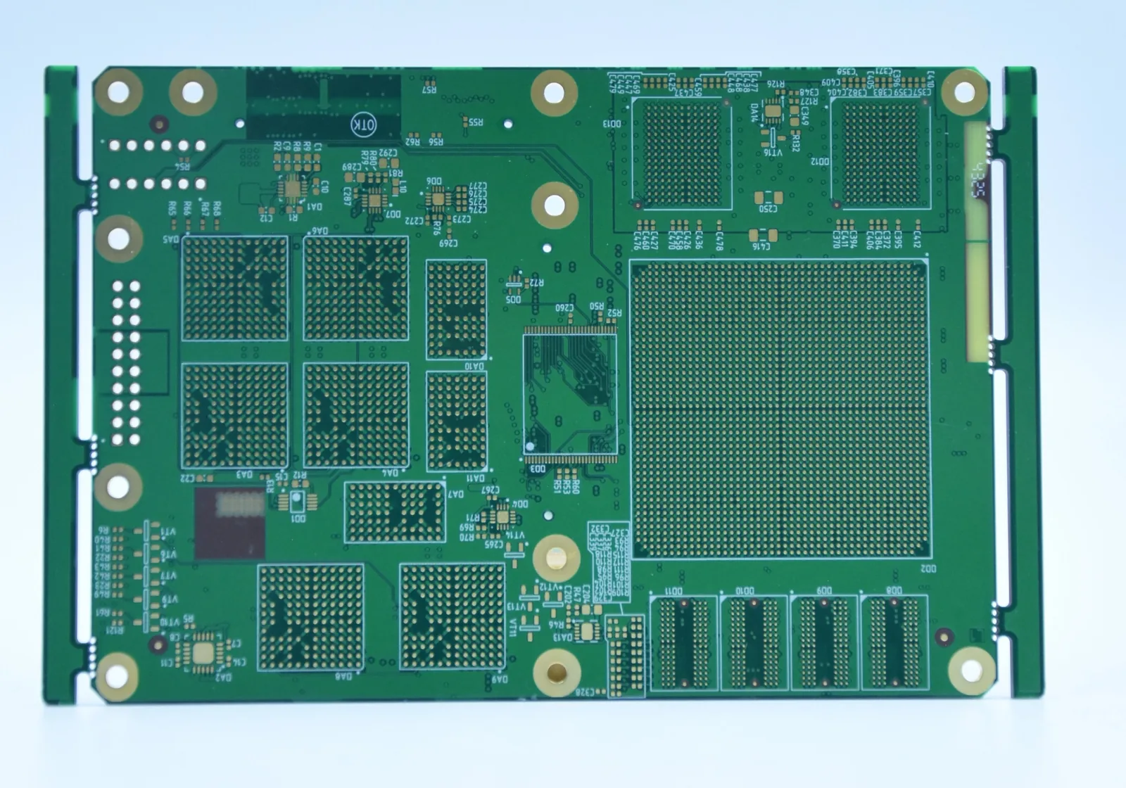
Dense impedance-controlled RF and datalink boards for airborne terminals.
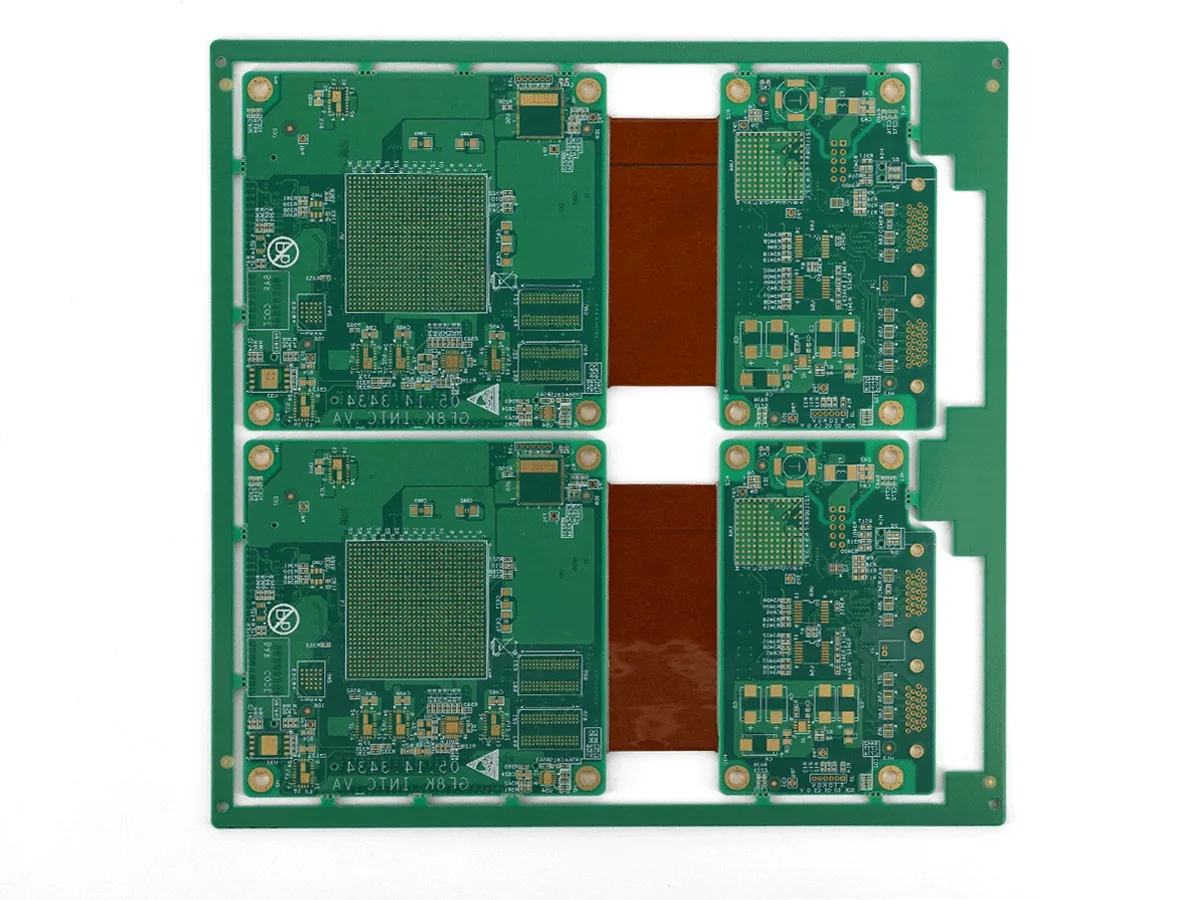
High-channel-count imaging modules where board area is the hard constraint.
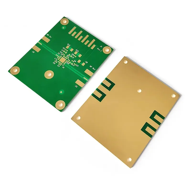
Low-loss mixed-material boards for massive-MIMO radio units.
What each BGA pitch band demands in via type, line width and stack-up, from 1.0 mm down to 0.35 mm.
Read article
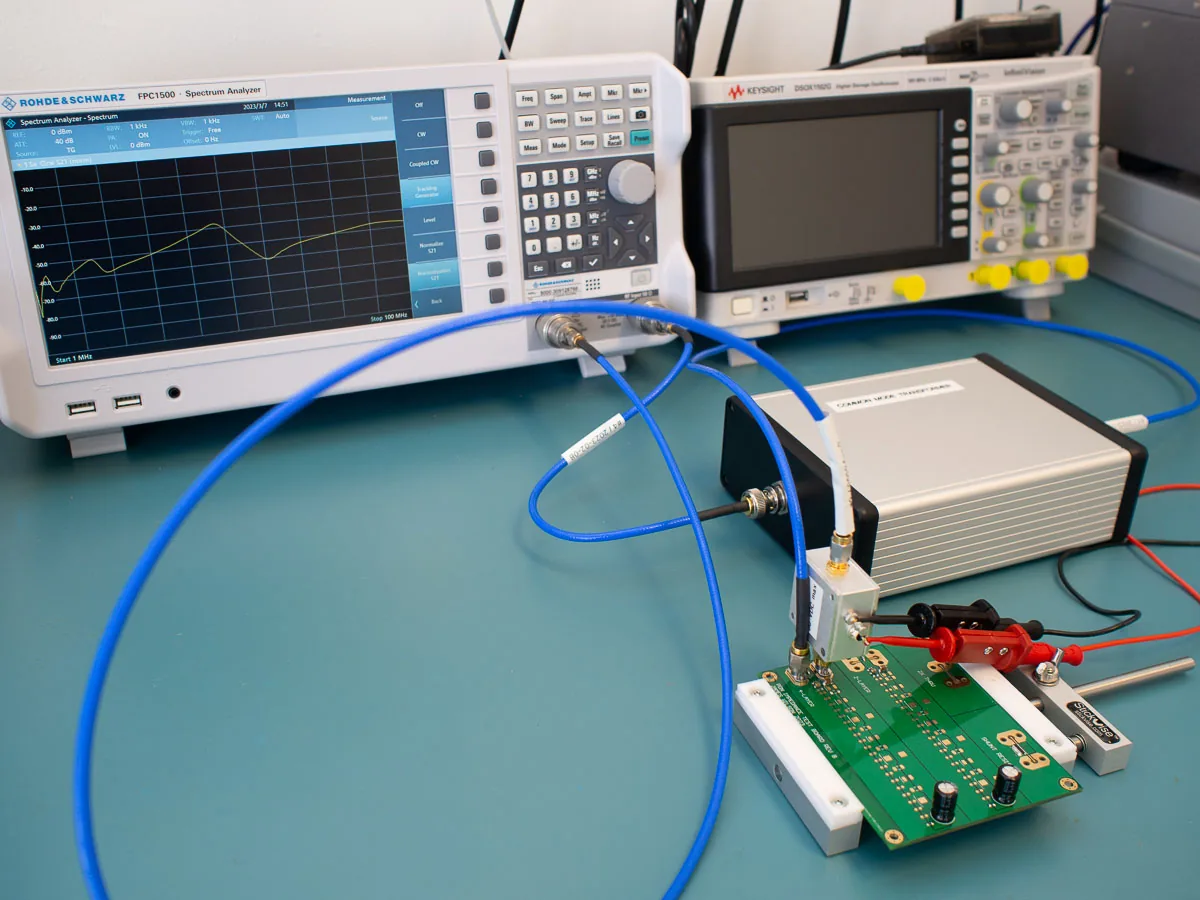
Four tolerances, four sensitivities, and why the root-sum-square lands at 7.1% while the worst case reaches 12%.
Read article
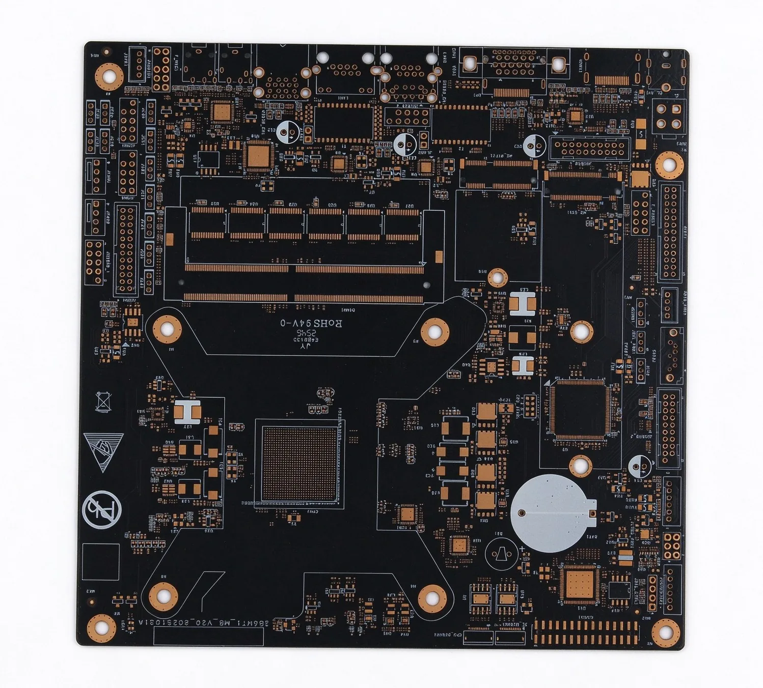
Six finishes on flatness, shelf life and cost, and the two questions that remove four of them immediately.
Read article
Laser microvias down to 0.1 mm; mechanical holes from 0.15 mm. Your practical minimum also depends on dielectric thickness and target pad size, which the CAM review confirms before tooling.
Any-layer builds are planned inside four cycles, with registration budgeted for every press. If the routing needs more, we test whether a staggered arrangement or a different layer count solves the same escape with fewer laminations.
TDR coupons run with every production panel: ±5% standard, ±3% on request. The measured data travels with the CoC, and a lot outside the window is held for engineering disposition rather than shipped.
Gerber RS-274X or ODB++, drill and via files, plus a stack-up drawing if one exists. If the via strategy is still open, tell us the escape pitch and we will propose one.
Lead time is confirmed at quotation for the specific stack-up and cycle count, with expedited options available. If the schedule moves, we tell you when we know — not on the ship date.
That is the work we are set up for. Quote in 24 hours.