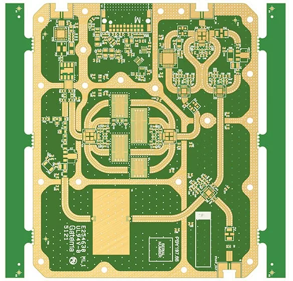
Heavy Copper Design Rules: Current, Etch and Thermal Vias
At 3 oz the etchant travels sideways through 105 µm of copper, so the minimum space opens to 0.20 mm and the trace section becomes a trapezoid.
Read article

Copper from 4 oz to 12 oz — traces that carry the current directly and spread the heat, then still hold their line width after etching and their flatness after lamination.
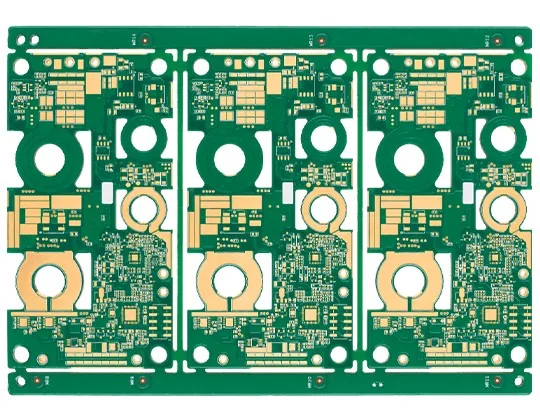
A heavy copper PCB swaps the standard 1 oz foil — about 35 µm — for 4 oz up to 12 oz, roughly 140 µm to 420 µm. The weight is not the point: a thicker trace carries more current with less voltage drop and less self-heating, spreads heat away from hot components, and can replace several parallel thin layers with one direct high-current path.
Plenty of shops treat heavy copper as a thickness setting. The order runs on the standard etch and lamination recipe, and the consequences surface later as undercut traces, resin-starved corners and copper that varies across the panel. Thick copper is a process problem, and it is solved before the first panel is made.
At HSX CIRCUIT the copper weight drives the whole route: pre-compensated artwork per weight and line class, prepreg fill calculated for the copper volume, thermal via and copper-fill design under the heat sources, and high-current verification at the end. 80 CAM engineers review 6,000+ designs every month; heavy-copper files get a first engineering pass within 24 hours, before artwork is committed.
Side-etch does not scale linearly with copper weight. Artwork is pre-compensated per weight and line class, first-article cross-sections confirm the finished trace, and the minimum line and space for that build are agreed before release instead of discovered afterwards.
Thick copper leaves cavities that resin has to fill without starving the prepreg. Fill volume is calculated per stack-up, prepreg grades are chosen for it, and pressure is staged so the panel stays uniform in thickness and no void survives at a copper edge.
Heat has to leave the device, not linger in the trace. Thermal vias sit directly under the heat source, are copper-filled and planarised where the pad must stay flat, and are plated to a controlled wall thickness so the path from component to inner copper or heatsink stays continuous.
A heavy-copper board is only as good as its resistance path. Four-wire resistance, high-current load and thermal imaging compare the measured ΔT with design intent, and cross-sections confirm copper thickness where it matters. 100% electrical test still closes the line.
| Parameter | Capability |
|---|---|
| Outer copper | 0.5–6 oz standard; 12 oz on inquiry |
| Inner copper | 0.5–4 oz |
| Min trace / space | 0.075 mm / 0.075 mm on thin copper; agreed per weight on 4 oz and above |
| Board thickness | 0.4–6.0 mm |
| Layer count | 2–32 layers standard; 50+ on inquiry |
| Max panel size | 600 × 900 mm |
| Thermal vias | Copper-filled and planarised; via-in-pad on request |
| Electrical test | 100% — flying probe (prototype), fixture (volume) |
UL 94 V-0 · IPC-6012 / IPC-A-600 · IPC Class 2 standard, Class 3 on request · Full matrix: see Capabilities.
Send the files before layout is frozen — etch compensation is cheaper to agree than to re-spin.
Inverter and battery-management boards that carry pack current on the board itself.
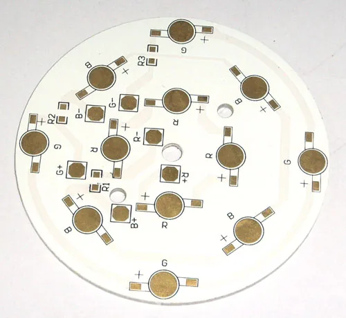
Power stages where heavy copper and a metal base together move heat out of the switching devices.
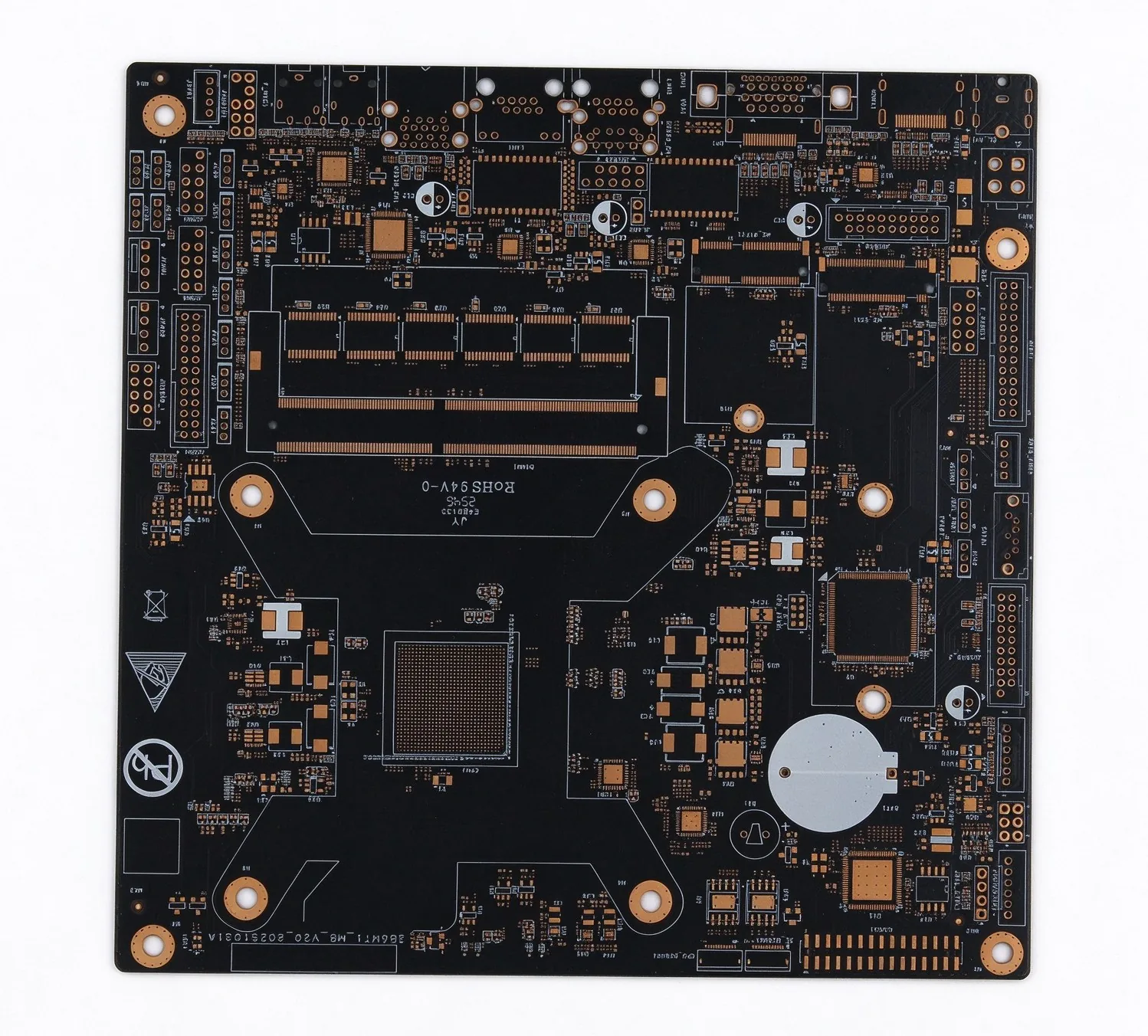
High-current output stages with thermal vias and thick inner layers for a short, low-loss return.
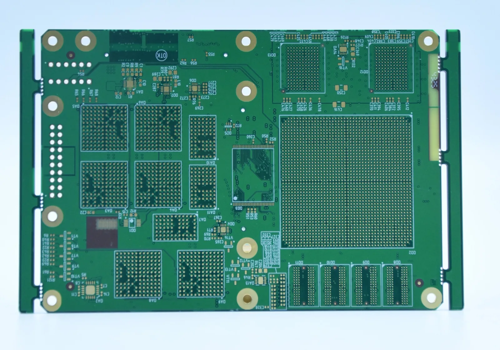
Distribution and protection boards that replace cable harnesses with etched copper.
At 3 oz the etchant travels sideways through 105 µm of copper, so the minimum space opens to 0.20 mm and the trace section becomes a trapezoid.
Read article
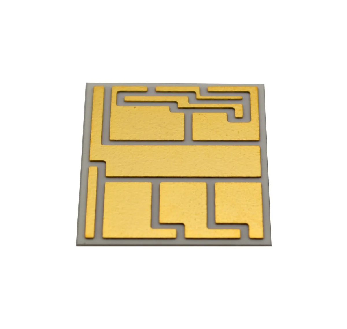
Alumina at 20–24 W/m·K and AlN at 170 against 0.2–0.3 for FR-4, plus the crossover arithmetic that decides which one ships.
Read article
The dielectric sets the thermal limit, not the aluminium: about 0.050 °C/W at 100 µm and 2 W/m·K under a 10 cm² source.
Read article
Yes, up to 12 oz outer copper on inquiry; 4–6 oz is standard production. A 12 oz design is reviewed for etch compensation, prepreg fill and via plating before it is quoted, so lead time and yield are confirmed rather than assumed.
Copper thickness. Etching removes material sideways as well as down, so a 6 oz trace needs more pre-compensation than a 1 oz trace, and spacing has to let the etchant reach the gap. Minimum line and space are quoted per copper weight; thin copper still runs to 0.075 mm.
Start at the heat source: thermal vias directly under the device, copper-filled and planarised so the pad stays flat, connecting to inner copper planes or the base. Then size the copper area and state the ΔT you need. We verify the path with thermal imaging before shipment.
Gerber (RS-274X) or ODB++, drill and outline files, copper weight per layer, stack-up if you have one, and the current each trace must carry. Upload through the quote page; a CAM engineer reviews the files within 24 hours.
Lead time is confirmed at quotation. Heavy copper depends on foil availability and the number of lamination cycles, so the date is set with the quote and any change is raised in writing rather than absorbed silently.
Send the current and the files. Quote in 24 hours.