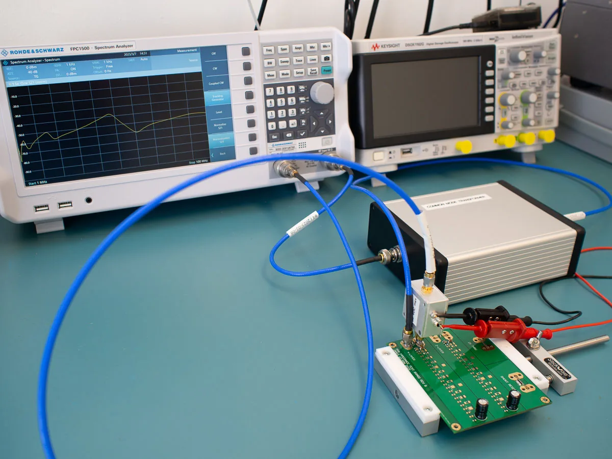
Controlled Impedance Tolerances: ±5% versus ±10%
Four tolerances, four sensitivities, and why the root-sum-square lands at 7.1% while the worst case reaches 12%.
Read article

High-speed boards where impedance is engineered into the stack-up before the first panel is imaged — coupon-correlated on every lot, back-drilled where the stub matters, and an engineering answer back within 24 hours.
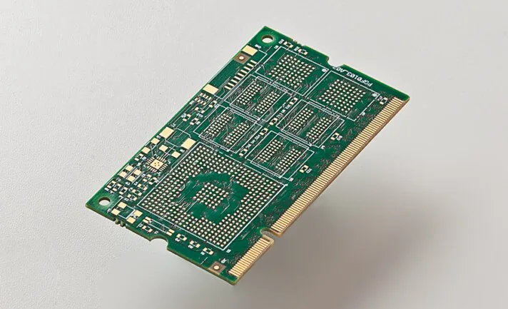
A board becomes a high-speed board at the moment its signal rise time is short enough that a trace stops behaving like a wire and starts behaving like a transmission line. From there, three things decide whether the channel survives: signal integrity, controlled impedance, and dielectric loss. The same design above roughly 3 GHz is usually called a high-frequency PCB — the physics has not changed, but skin effect, dispersion and laminate Df now dominate, and the material moves from FR-4 to low-loss or PTFE-class laminate.
Many factories sell high-speed as a material label: swap in a low-Dk laminate, print the grade on the traveller, ship. A laminate alone does not fix a channel. What fixes it is the stack-up — which layer is the reference plane, how far the dielectric sits under the trace, how wide the line etches after compensation, and how much stub is left inside every through via. At HSX CIRCUIT we treat high-speed as stack-up and impedance engineering, and the laminate is the last decision rather than the first.
80 CAM engineers review 6,000+ unique designs every month, and a high-speed order is not released to the line until the stack-up has been modeled, the impedance targets have been matched to a coupon pattern, and the back-drill depth has been calculated for each via span. Every production panel carries a TDR coupon measured against those targets, and measured values ship with the CoC — ±5% standard, ±3% on request. Software is not the differentiator here; the coupon, the cross-section and the disposition rule are.
Impedance traces are modeled against the dielectric thickness and copper weight actually present in the build, never against a generic table. The stack-up drawing comes back with target line widths before the first panel is imaged, so what you approve is what gets etched.
MEGTRON-class and high-Tg laminates are matched to the loss budget at the frequency where the channel really runs. Dk shift from resin content and glass weave is folded back into line width — a datasheet Dk is not an impedance target by itself.
A through via leaves a stub that resonates and closes the eye at high data rates. Back drilling is depth-controlled to ±0.05 mm per span and verified on cross-section, so residual stub stays inside what the channel can tolerate.
A coupon is only useful if it is measured the same way every time. Impedance coupons sit on every production panel, are read by TDR, and any lot outside the agreed window — ±5%, or ±3% where specified — is held for engineering disposition instead of shipped with a note.
| Parameter | Capability |
|---|---|
| Impedance tolerance | ±5% standard, ±3% on request; TDR coupon on every panel, measured values ship with the CoC |
| Back drilling | Depth control ±0.05 mm per via span; residual stub confirmed on cross-section |
| Layer count | 2–32 layers standard; 50+ on inquiry (sequential lamination) |
| Min trace / space | 0.075 mm / 0.075 mm |
| Materials (Dk / Df) | FR-4 class Dk 4.2–4.6, Df 0.015–0.020; low-loss Dk 3.4–4.0, Df 0.002–0.005 (at 1 GHz) |
| Board thickness | 0.4–6.0 mm |
| Drill / registration | Mechanical from 0.15 mm, laser from 0.1 mm; layer-to-layer registration ±50 µm |
| Electrical test | 100% — flying probe on prototypes, fixture on volume builds |
UL 94 V-0 · Built to IPC-6012 / IPC-A-600 · IPC Class 2 standard, Class 3 on request · Full matrix: see Capabilities.
Send Gerbers and your impedance targets — a CAM engineer answers, not a form.
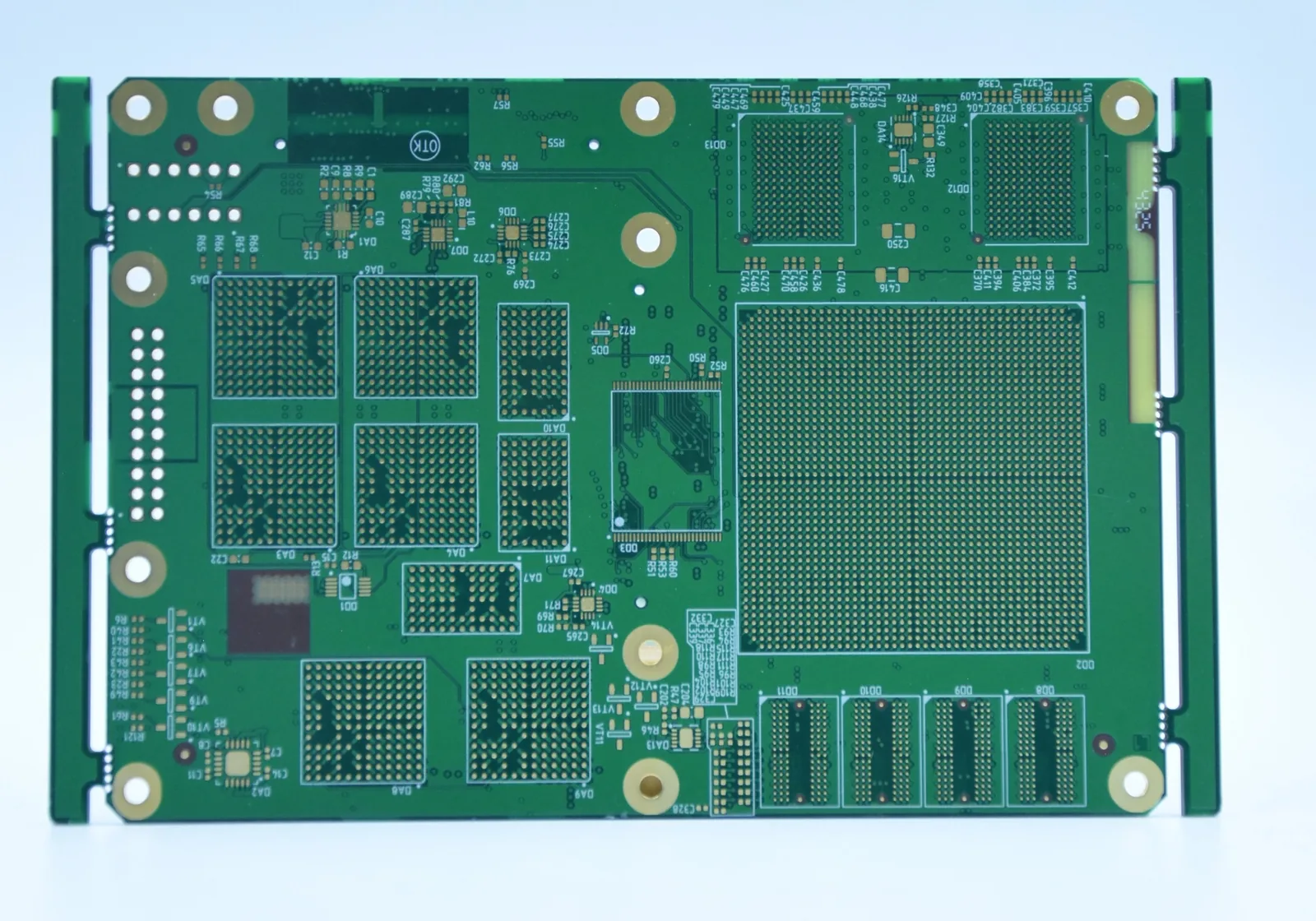
24-layer backplanes with back-drilled vias, 100 Ω differential pairs and long-reach traces.
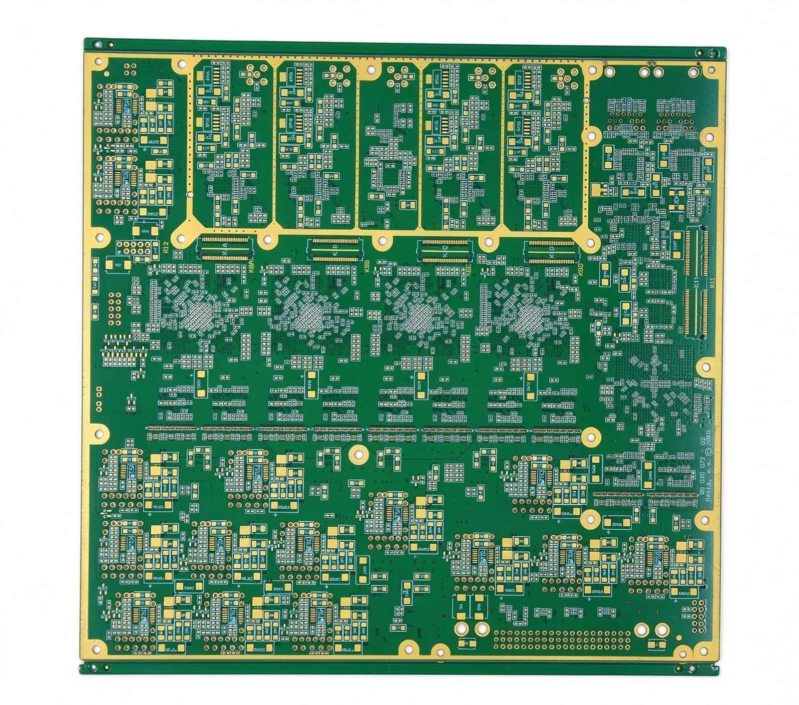
Fine-line HDI server boards where dense routing and controlled impedance share one panel.
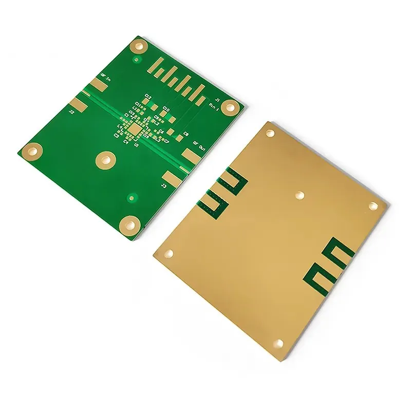
Low-loss and Rogers hybrid radio units running above 6 GHz with strict Dk stability.
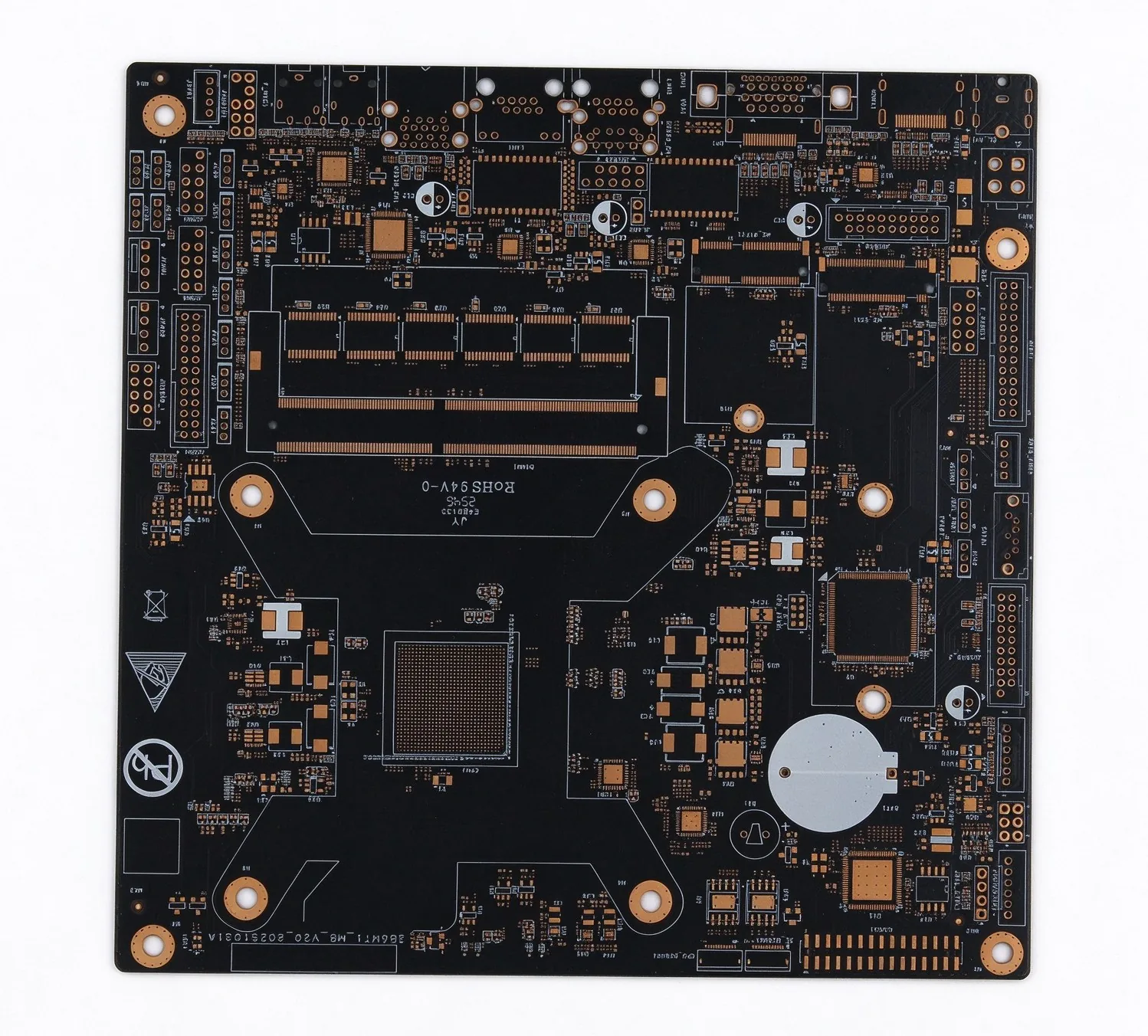
Instrumentation where a 5% impedance error shows up as a visible measurement error.
Four tolerances, four sensitivities, and why the root-sum-square lands at 7.1% while the worst case reaches 12%.
Read article
A residual stub notches the channel at 36 GHz per millimetre on FR-4, so drill depth is a channel-budget decision before it is a process one.
Read article
Two resin systems through one press cycle, a 190 °C compromise profile, and why desmear behaves differently on each plastic.
Read article
±5% covers most 100 Ω differential and 50 Ω single-ended channels at standard price. ±3% is specified when channel margin is thin — longer traces, higher data rates, or a receiver already close to its eye limit. Tightening the window changes the line-width allowance and the coupon sampling, so it is quoted per design rather than promised on every order.
The coupon is a test trace built into the panel border with the same line width, dielectric and layer stack as the real channels. It is read by TDR and compared with the modeled target; the measurement ships with the CoC, and a lot outside the agreed window is held for engineering disposition rather than released.
Depth control is ±0.05 mm per via span, so the achievable residual stub follows your layer span and board thickness rather than a single fixed number. We calculate it for each span during engineering review and tell you plainly when the target is not reachable on the stack you sent.
Start from the loss budget at the frequency the channel actually runs, then take the lowest-cost laminate that meets it. Below about 3 GHz a high-Tg FR-4 is usually enough; at 10 Gbps and above a low-loss MEGTRON-class laminate or a Rogers hybrid stack is normally required. High-frequency and high-speed are used almost interchangeably — the laminate follows the loss number, not the label.
Lead time is confirmed at quotation. It depends on laminate availability, layer count and whether back drilling is in scope; the date is stated with the quote, and any material that has to be ordered in is flagged before the order is placed.
That is the build we are set up for. Quote in 24 hours.