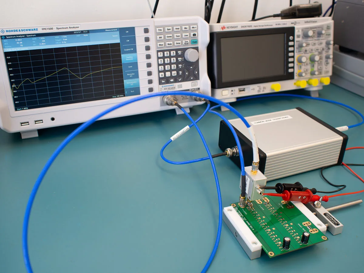
Controlled Impedance Tolerances: ±5% versus ±10%
Four tolerances, four sensitivities, and why the root-sum-square lands at 7.1% while the worst case reaches 12%.
Read article

A via is a transmission line down to the layer it serves and an open stub below it, and the stub’s first notch is predictable before the board is drilled. That makes back-drilling an arithmetic question first and a drilling question second — the process only has to deliver a depth the channel already asked for.
A via carries a signal from the top layer to the layer it needs, and the plated barrel keeps going below that layer to the bottom of the board. The lower section is not on the drawing, but it is in the circuit: it ends open at the far end of the barrel and reflects whatever arrives at it. At the quarter-wave frequency the round trip is half a wavelength, the reflection comes back in antiphase, and the channel shows a notch.
The frequency is fixed by geometry rather than by the driver: f = c / (4 · L · √Dk), with L the residual stub and Dk the laminate the stub sits in. On FR-4 at Dk 4.35 that works out to 36 GHz per millimetre, so a 1.0 mm stub notches at 35.9 GHz, 0.5 mm at 71.8 GHz, and 0.25 mm at 143.6 GHz. The same length on Rogers 4350B notches about 9% higher, because Dk is what sets the wavelength.
| Residual stub | First notch, FR-4 Dk 4.35 | First notch, Rogers 4350B Dk 3.66 |
|---|---|---|
| 2.0 mm | 17.9 GHz | 19.6 GHz |
| 1.0 mm | 35.9 GHz | 39.2 GHz |
| 0.5 mm | 71.8 GHz | 78.4 GHz |
| 0.25 mm | 143.6 GHz | 156.8 GHz |
| 0.15 mm | 239.3 GHz | 261.4 GHz |
Computed with f = c / (4 · L · √Dk), c = 300 mm/ns, √Dk 2.09 for FR-4 at 4.35 and 1.91 for 4350B at 3.66. First notch only; the second sits at three times the frequency and rarely matters before dielectric loss takes over.
What decides whether a stub matters is how close its notch sits to the band the channel actually uses. NRZ puts the Nyquist at half the bit rate; PAM4 puts it at a quarter, because the symbol rate is half the bit rate and the Nyquist is half of that. A 112G PAM4 link therefore reaches 28 GHz — the same band a 56G NRZ link would reach, at twice the throughput per pair.
The working rule is to keep the first notch at least twice the Nyquist, which leaves the notch outside the band with room for the second harmonic of the transition. Applied at Dk 4.35 that gives the stub limits below. They are limits for a through via from the top layer to the layer the net uses — a backplane via that runs from L1 to L20 has far more stub than the table allows — the case we build on high-speed boards, which is where the drill comes in.
| Interface | Bit rate / baud | Nyquist | Stub that keeps the notch above 2× Nyquist |
|---|---|---|---|
| 10G NRZ | 10 Gb/s | 5 GHz | 3.6 mm |
| 25G NRZ | 25 Gb/s | 12.5 GHz | 1.4 mm |
| 56G PAM4 | 56 Gb/s / 28 GBd | 14 GHz | 1.3 mm |
| 112G PAM4 | 112 Gb/s / 56 GBd | 28 GHz | 0.64 mm |
Stub limit = 35.9 / (2 × Nyquist) mm at Dk 4.35. The 2× rule is a design guard band for the transition band, not a standard; a channel with a clean eye and short reach can run with the notch closer.
The table explains why back-drilling arrives with 112G and not with 10G. On a 1.6 mm board a through via from L1 to L2 leaves a stub of roughly 1.4 mm, which at 10G sits far above the 5 GHz Nyquist and at 112G sits inside the band. Nothing changed in the drilling department; the channel moved.
Back-drilling runs a slightly larger bit into the finished via from the opposite side, down to a set depth, and cuts away the plated barrel below the layer that carries the signal. The bit is typically 0.15 to 0.20 mm larger than the signal drill so it clears the barrel wall without touching the target pad, and the depth is referenced to the board surface on the drill side.
Two tolerances decide whether it works. The first is depth: the residual is whatever the depth leaves behind, so a ±0.05 mm depth window is a ±0.05 mm stub window before anything else is counted. The second is registration — the bit has to stop inside the clearance of the target layer’s pad, and layer-to-layer registration is ±50 µm on our process, which is the number the annular clearance has to cover.
The operation also changes what the via looks like in cross-section: the barrel now ends partway through the board, the hole below it is wider than the signal hole, and the plating on the wall is interrupted at the transition. That is expected, and it is why the acceptance evidence is a slice rather than a drawing.
The numbers we publish for this operation are narrow on purpose, because a depth window is the only thing the customer can check without a cross-section:
Depth control is quoted as a window because the depth is referenced to a surface that has its own tolerance: panel thickness, press variation and copper distribution all move the surface the drill starts from. A drill program that is exact on paper still lands inside a window on the panel, and the window is what gets published.
Back-drilling is priced by drilling operations, not by board area. Every distinct depth is a separate setup: tool change, program, first-article check, and a slice to prove the depth before the panel runs. A design with one back-drill depth on a panel is cheap per hole; the same hole count split across four depths is four times the setup for the same copper removed.
| Driver | What it does to cost | Cheaper move |
|---|---|---|
| Distinct back-drill depths | One setup, tool and first-article slice per depth | Consolidate depths across the panel |
| Back-drilled holes per panel | Scales with hole count, not with area | Back-drill only the nets whose notch is in band |
| Residual stub target | Tighter depth window means more slice checks | Hold the target the Nyquist needs, not the tightest one available |
| Panel thickness spread | Depth referenced to surface, so spread eats the window | Control the press and measure thickness per lot |
| Aspect ratio above 12:1 | Tool deflection and depth control both get harder | Ask before designing the via, not after |
The cost list is ordered by how often it is the dominant term on a real quote: depth groups first, hole count second, everything else after.
The cheapest lever is usually in the stack-up rather than in the drill. Moving a critical net from the bottom of the board to the layer next to the top turns a 1.4 mm stub into a 0.1 mm one at no process cost, and consolidating four depths into two removes half the setup before a single hole is drilled.
Back-drilling removes a resonance; it does not restore loss. Dielectric and copper loss stay exactly where they were, so a channel that fails on loss will still fail after the barrel is cut. The operation is worth paying for when the notch is the problem, and the notch is identifiable from the stub length before anything is fabricated.
Three alternatives compete with it. Routing the net on the layer adjacent to the outer layer removes the stub by construction. Blind and buried vias remove it by building the via only as deep as it needs to go, at the cost of sequential lamination cycles — four is our standard ceiling, more goes to engineering review. A thinner board section does the same arithmetic with less process, as long as the stack still supports the impedance target.
The one thing that does not work is specifying back-drilling as insurance. A 0.15 mm residual on a 10G channel buys nothing that the 3.6 mm limit did not already allow, and it puts a depth group, a slice and a setup on the quote for a notch that sits 7× above the band.
A VNA sweep shows the notch directly: sweep to at least twice the highest notch of interest and look for the dip, not just the insertion loss at the band centre. A TDR shows the impedance profile and will show the stub as a capacitive excursion, but the notch frequency is easier to read from S21, which is why the coupon measurement and the simulation should use the same quantity.
Depth is verified by cross-section, and the section should come with three things: the depth actually achieved, the residual stub measured at that depth, and the panel position it was cut from. A slice from the panel centre proves the program; a slice from the edge proves the process, because that is where thickness and registration move first.
Ask for the slice on the first article rather than on the shipment. The residual stub is the only number that closes the loop between the drill program and the channel budget, and it is cheapest to change before the lot runs.
No. It pays when the first notch falls inside or near the band the channel uses. On a 1.6 mm board a through via from L1 to L2 leaves about 1.4 mm of stub, which is comfortable at 10G and inside the band at 112G PAM4. The data rate decides, not the word ‘high-speed’ on the drawing.
We hold back-drill depth to ±0.05 mm and confirm the residual on a cross-section, because depth is referenced to a surface that moves with panel thickness and press variation. The drawing states a target; the slice states what the panel actually has.
The risk is mechanical rather than electrical: the bit has to clear the barrel without clipping the target layer’s pad, so annular clearance has to cover layer registration of ±50 µm. First-article slices catch a program that stops short or runs deep before the lot does.
Blind and buried vias remove the stub by construction, but they add sequential lamination cycles — four is our standard ceiling. Back-drilling is one extra drilling operation on a through via, which is cheaper when the stack is simple and the stub is the only problem.
No. The stub creates a notch near its quarter-wave frequency; loss comes from the dielectric and the copper. Remove the notch and the loss curve stays where it was, so a channel that fails on loss needs a different laminate or a shorter route, not a drill.
Four tolerances, four sensitivities, and why the root-sum-square lands at 7.1% while the worst case reaches 12%.
Read article
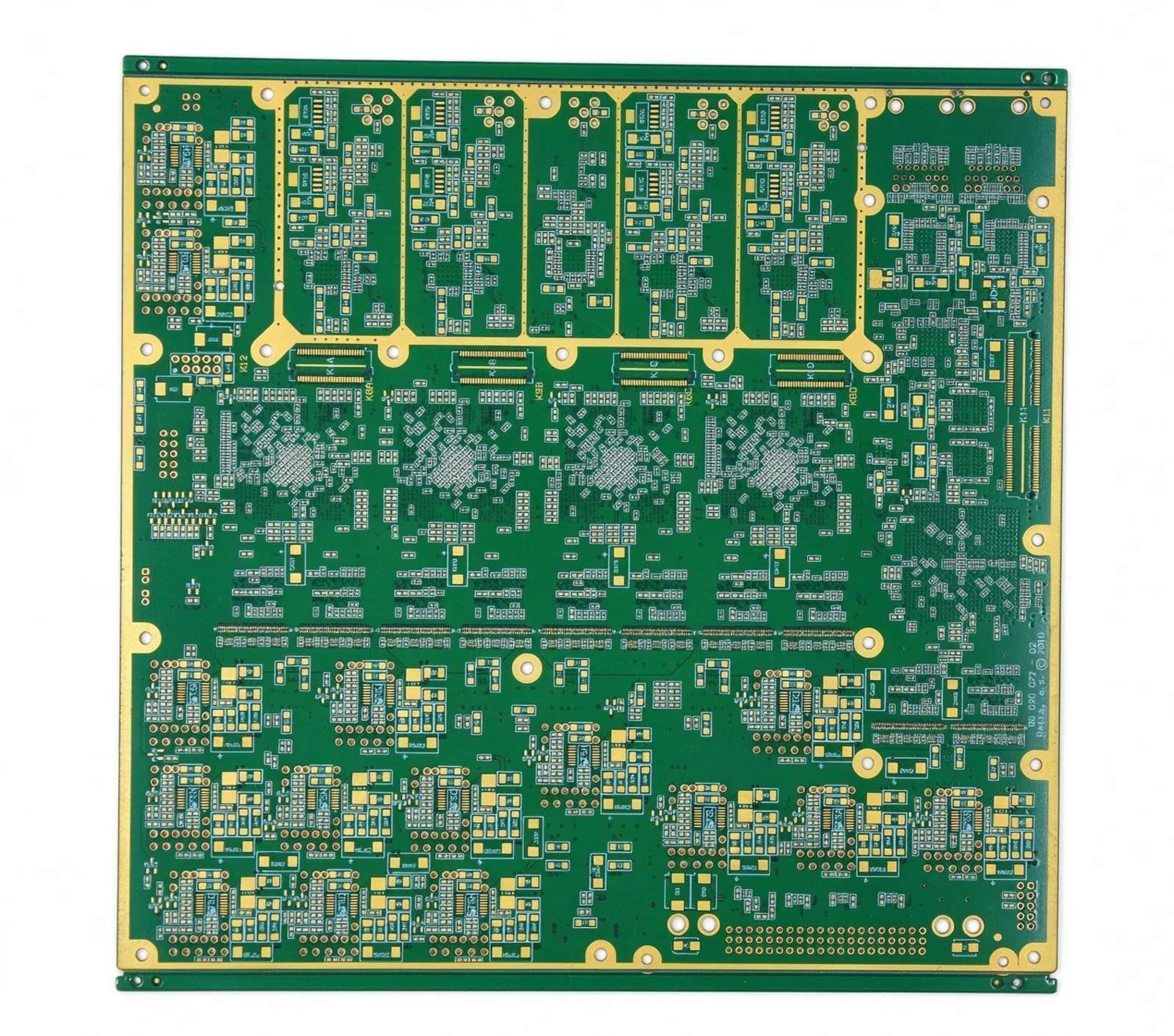
What each BGA pitch band demands in via type, line width and stack-up, from 1.0 mm down to 0.35 mm.
Read article
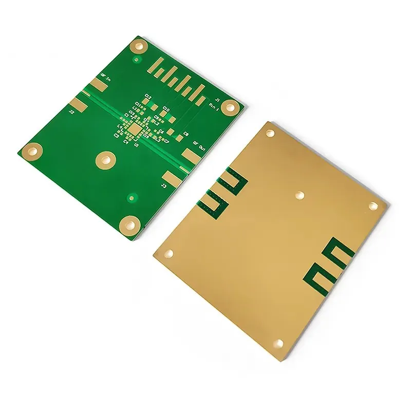
Two resin systems through one press cycle, a 190 °C compromise profile, and why desmear behaves differently on each plastic.
Read article
Send the stack-up with the data rate and the layer each critical net uses. Quote in 24 hours, with the stub target named per via. Every build runs to IPC Class 2 standard, Class 3 on request.