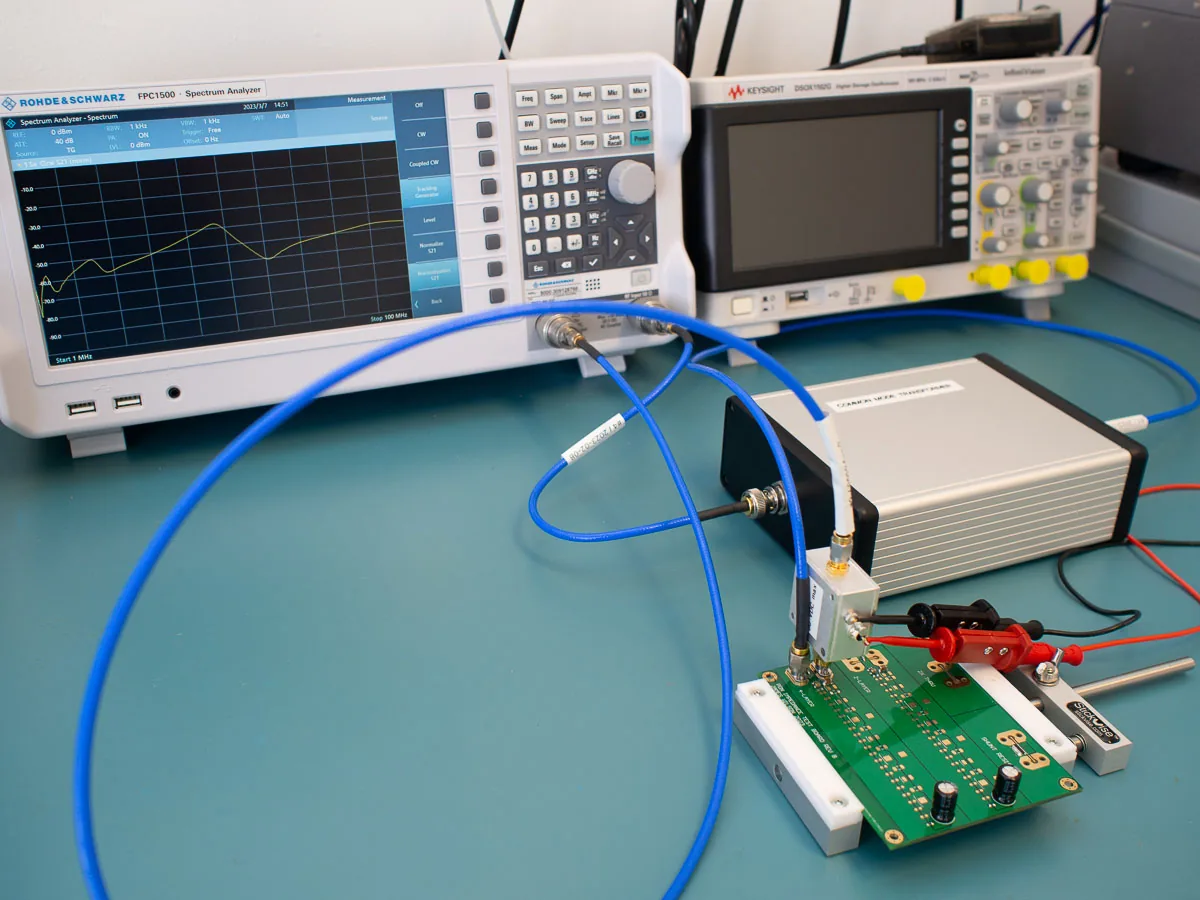
Controlled Impedance Tolerances: ±5% versus ±10%
Four tolerances, four sensitivities, and why the root-sum-square lands at 7.1% while the worst case reaches 12%.
Read article

Pitch decides the escape before the stack-up exists. A 1.0 mm part routes with a mechanical drill and a dogbone; a 0.4 mm part needs a laser via inside the land and 0.075 mm lines. The bands below give the via type, the line width and the stack-up for each pitch, with the arithmetic that shows why the boundary sits where it does.
The space between two adjacent BGA lands is the pitch minus the land diameter, and that gap has to hold one trace plus two clearances. At 0.8 mm pitch with a 0.45 mm land the gap is 0.35 mm, enough for a 0.15 mm line with 0.10 mm on each side. At 0.5 mm pitch with a 0.28 mm land the gap is 0.22 mm, which fits a 0.10 mm line with 0.06 mm clearance. At 0.4 mm pitch with a 0.20 mm land the gap is 0.20 mm, so the line drops to 0.075 mm.
That arithmetic is why the via type follows the pitch rather than leading it. A dogbone puts the via beside the land, which costs lateral space the channel does not have. Once the gap falls below about 0.25 mm the dogbone consumes the routing channel and the via has to move inside the land. The real boundary between through-via and microvia designs sits between 0.8 mm and 0.65 mm, regardless of how many layers the board carries.
At 1.0 mm pitch a 0.30 mm mechanical drill with a 0.60 mm land leaves 0.40 mm of channel, which carries 0.20 mm line and space comfortably. At 0.8 mm a 0.25 mm drill with a 0.45 mm land still leaves 0.30 mm, and a dogbone can sit in the channel because the escape only needs one route per row. Boards in this band use conventional multilayer lamination with no sequential steps, and they are quoted as ordinary multilayer work.
The band ends when the dogbone plus the trace no longer fit, which happens around 0.65 mm. Below that, keeping through vias forces the escape to drop layers at every row, and the layer count climbs faster than the pitch shrinks. That is the economic argument for HDI, and it is not about via size: it is the routing density that lets a six-layer HDI replace a twelve-layer through-hole board.
At 0.65 mm pitch the land is 0.30 to 0.35 mm and the channel is the same, which still carries 0.125 mm line and space. Putting the microvia in the pad removes the dogbone from the channel and buys back roughly 0.10 mm — the difference between one trace per channel and none. Structures at this pitch are typically 1+N+1 with a single laser layer on each side.
At 0.5 mm the land drops to 0.25 to 0.30 mm and the channel to 0.20 or 0.25 mm. With a 0.28 mm land the gap is 0.22 mm, and a 0.10 mm line with 0.06 mm clearance consumes it exactly. There is no margin for a dogbone. Every via in the array sits in the pad, filled and capped, and the stack-up is 1+N+1 or 2+N+2 depending on how many layers the escape needs.
At 0.4 mm pitch the land is 0.20 to 0.25 mm, the gap is 0.20 mm, and the line drops to 0.075 mm — which is the floor of our standard subtractive process. At that width 35 µm copper etches with a trapezoidal cross-section and the top of the trace narrows below the design value, so the copper weight has to be chosen with the etch factor in mind rather than assumed. The escape needs two laser layers per side, the structure becomes 2+N+2, and the lamination count rises to three.
Below 0.075 mm the subtractive process runs out of control: side etch consumes an increasing fraction of the trace and the impedance spread widens with it. Modified semi-additive processing builds the trace by plating into a pattern instead of etching around it, which holds 0.05 mm line and space. At that point the pad ring budget becomes the binding constraint, not the routing channel. That is the domain of any-layer HDI, and it is quoted rather than published as a catalogue number.
| BGA pitch | Escape via | Line and space | Stack-up band |
|---|---|---|---|
| 1.0 mm | Through via, 0.30 mm drill, dogbone | 0.20 / 0.20 mm | Conventional multilayer |
| 0.8 mm | Through via, 0.25 mm drill, or one laser layer | 0.15 / 0.15 mm | Conventional or 1+N+1 |
| 0.65 mm | Microvia in pad, 0.10 mm | 0.125 / 0.125 mm | 1+N+1 |
| 0.5 mm | Microvia in pad, 0.10 mm | 0.10 / 0.10 mm | 1+N+1 or 2+N+2 |
| 0.4 mm | Stacked microvia in pad | 0.075 / 0.075 mm | 2+N+2 |
| 0.35 mm | Stacked microvia, mSAP lines | 0.05 / 0.05 mm | 2+N+2 or any-layer |
Land diameters and line widths are a typical industry window for each band; the channel arithmetic follows from pitch minus land. The stack-up band reflects the escape layers the pitch requires, not a fixed rule.
What costs money in a stack-up is the number of lamination cycles. A 1+N+1 build needs two, a 2+N+2 build needs three, and an any-layer build needs one cycle per laser layer. That is why a 0.5 mm pitch design on 2+N+2 is priced differently from a 0.65 mm design on 1+N+1 even when both come out at six layers total.
The practical method is to count the layers the escape needs, add the ground and power layers the design needs, and call the remainder the core. A 0.5 mm pitch BGA with 400 balls typically escapes in two signal layers per side, which gives 2+N+2 with a four-layer core. A 0.8 mm part with the same ball count escapes on one layer per side or with through vias on a conventional eight-layer board — and the conventional board is usually the cheaper answer.
| Cost checkpoint | Trigger | Effect |
|---|---|---|
| Sequential lamination | Two or more lamination cycles | 30–50% adder on the lamination steps only |
| Any-layer HDI | Every layer laser-drilled | Above 2+N+2; quoted per design |
| mSAP fine lines | 0.05 mm line and space | Process and volume dependent |
| Via fill and cap | Via in pad under a BGA | Per via count and panel area |
The sequential lamination adder applies to the press and drilling operations, not to the whole board price. Any-layer and mSAP adders depend on volume, so they are quoted rather than estimated from a factor.
The ring budget, not the channel. A 0.10 mm via with 50 µm of ring per side, minus ±40 µm of layer-to-layer registration, leaves 10 µm at the thinnest point — below any acceptance criterion worth writing. The channel can be recovered with narrower lines or more layers. The ring cannot be recovered without changing the aperture, the registration class or the dielectric thickness.
Acceptance follows IPC-6012: for boards over two layers the hole copper requirement sits at 25 µm average and 20 µm minimum, and microvias carry a separate requirement in the same standard. Registration is where we hold the line: ±50 µm layer to layer is the published figure, and the ring budget is checked against it at DFM review rather than discovered at cross-section.
One number worth knowing before layout: through-hole aspect ratio. Our standard is 12:1 on board thickness, with 20:1 on inquiry. A design that needs a 0.20 mm drill through a 3.2 mm board is asking for 16:1, which changes both the drill programme and the plating time — worth raising while the stack-up is still a spreadsheet.
Between 0.8 mm and 0.65 mm. At 0.8 mm a 0.25 mm through via with a dogbone still fits the channel; at 0.65 mm the dogbone consumes the space the trace needs, so the via moves into the pad. The crossover is set by the channel arithmetic, not by a supplier preference, which is why it lands in the same place across fabricators.
It is possible with 0.075 mm line and space and stacked microvias, which is a 2+N+2 build. The line width sits at the edge of subtractive etching, so impedance tolerance widens and copper weight has to be chosen with the etch factor in mind. Below 0.4 mm the line width leaves the subtractive window entirely.
1+N+1 needs two, 2+N+2 needs three, and any-layer needs one per laser layer. The adder applies to the lamination steps rather than to the whole board, so a three-cycle build is not proportionally more expensive overall — the extra cost sits in pressing and drilling.
In practice, yes. At 0.05 mm line and space, subtractive etching loses too much of the trace to side etch and the resulting impedance spread is wider than a controlled window allows. Modified semi-additive processing plates the trace into a pattern and holds the width, at a cost that scales with volume.
Four tolerances, four sensitivities, and why the root-sum-square lands at 7.1% while the worst case reaches 12%.
Read article
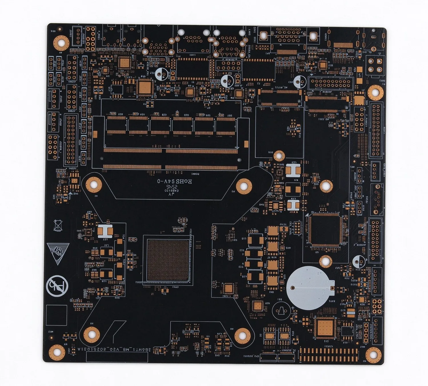
Six finishes on flatness, shelf life and cost, and the two questions that remove four of them immediately.
Read article
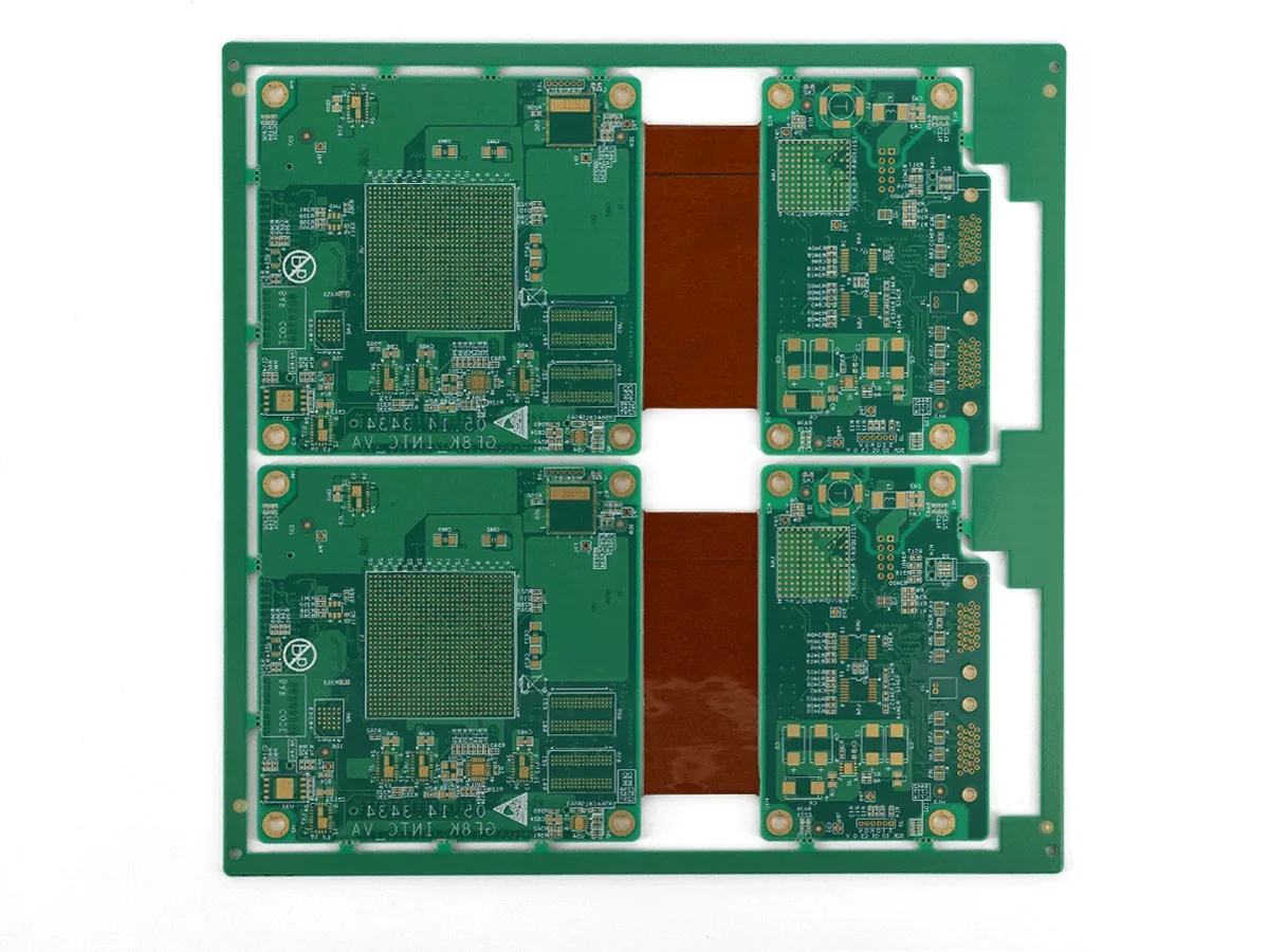
Three configurations, five cost drivers, and the interconnect count that decides whether the rigid premium comes back.
Read article
Send the Gerbers and the stack-up. Quote in 24 hours, with the cycle count and registration class written into it. Every build runs to IPC Class 2 standard, Class 3 on request.