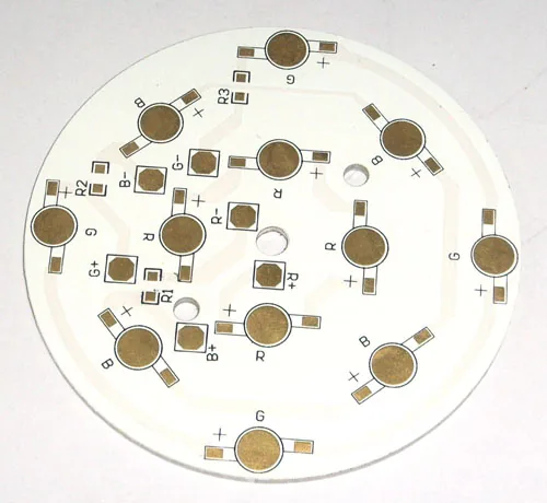
Metal Core LED Layout: Thermal Pad and Isolation Rules
The dielectric sets the thermal limit, not the aluminium: about 0.050 °C/W at 100 µm and 2 W/m·K under a 10 cm² source.
Read article

A ceramic substrate beats FR-4 on conductivity by two orders of magnitude and on dielectric loss by one — and still loses most of the time, because the gap only pays where heat is concentrated. Start from flux density at the die, not from material names.
Conductivity is a material property; what decides a design is watts per square centimetre at the hottest seat. Spread two watts over a hundred square centimetres and any substrate works. Put twenty watts on one square centimetre and the laminate term alone becomes tens of degrees per watt — at which point the substrate is no longer packaging, it is the heat sink.
So the first number to find is flux density at each die seat, not the average across the board. The second is frequency, and the third is volume. Those three place the design in one of five bands, and only two of them are ceramic.
| If the board… | Choose | What to check next |
|---|---|---|
| Concentrates more than about 5 W/cm² at die seats | Ceramic, AlN first above 10 W/cm² | Die-attach stress and CTE |
| Runs RF or fast edges past 5–10 GHz on long lines | Ceramic or low-loss laminate | Loss budget at the named frequency |
| Cycles −40 to +125 °C with large direct-attached dies | Ceramic, AlN preferred | In-plane CTE against silicon |
| Dissipates under about 1 W/cm², cost-sensitive, volume | FR-4 | Nothing below challenges it |
| Needs six or more routing layers with fine mechanics | FR-4 | Ceramic multilayer is a quoted special process |
| Has one hot seat on an otherwise mild board | FR-4 plus metal core | Step up only as far as the budget needs |
Bands are industry-typical by flux, frequency and volume. Ceramic is not one material: alumina and AlN differ by roughly seven times in conductivity, so the grade has to be named before the comparison means anything.
Conductivity removes heat in Z and spreads it in plane, and the two jobs pay differently depending on die size. The comparison only works at one temperature and one stated thickness, because resistance is thickness divided by conductivity — a thin high-conductivity substrate and a thick low-conductivity one can land in the same place.
| Parameter | Alumina 96% | AlN | FR-4 class | Basis |
|---|---|---|---|---|
| Conductivity | 20–24 W/m·K | 170 W/m·K and above | 0.2–0.3 W/m·K | Bulk, 25 °C |
| Normalised resistance | 0.26–0.32 °C·cm²/W at 0.63 mm | 0.032–0.037 °C·cm²/W at 0.63 mm | ≈64 °C·cm²/W at 1.6 mm | Thickness ÷ conductivity |
| Thickness grades | 0.25 / 0.38 / 0.63 / 1.0 mm | 0.38 / 0.63 / 1.0 mm | 0.4–6.0 mm | Standard stock |
Resistance figures follow directly from thickness over conductivity at 0.25 W/m·K for FR-4 and 24 W/m·K for the 96% alumina grade we quote. Change the laminate or the thickness and the row changes with it.
The arithmetic is what settles arguments. Twenty watts on one square centimetre through 1.6 mm of FR-4 is about 64 °C/W of substrate alone; the same heat through 0.63 mm of AlN is 0.32 °C/W. Two watts over a hundred square centimetres through the same FR-4 adds roughly 1.3 °C — which is why a mild controller never pays for ceramic, whatever the conductivity ratio says.
In-plane expansion stresses an attached die; expansion through the thickness works the via barrels. Quoting one CTE number without the axis makes the comparison meaningless, and it is the most common way a substrate datasheet misleads a design review.
| Material | In-plane CTE | Z-axis CTE | Natural match | What to watch |
|---|---|---|---|---|
| Silicon die | ≈3 ppm/°C | ≈3 ppm/°C | — | Reference |
| AlN | 4–5 ppm/°C | 4–5 ppm/°C | Silicon | Brittle handling |
| Alumina 96% | 6–7 ppm/°C | 6–7 ppm/°C | Ceramic packages | Die-attach stress against silicon |
| FR-4 class | 14–17 ppm/°C | 45–70 ppm/°C, split at Tg | Copper at 17 | Barrel fatigue in Z |
| Copper | ≈17 ppm/°C | ≈17 ppm/°C | FR-4 in plane | — |
In-plane values over 20–100 °C. FR-4 expands differently below and above Tg, so its Z figure is a range across the transition rather than one number.
AlN at 4–5 ppm/°C against silicon at 3 keeps joint strain low through thermal cycling, which is the real reason it appears in automotive power modules rather than the conductivity alone. FR-4 sits close to copper in plane, which is why its failures collect in the Z axis at the barrels rather than at the die attach.
Dielectric constant and loss tangent are labelled by frequency and by method. A table that puts ceramic at 1 MHz beside FR-4 at 1 GHz is comparing two different measurements, not two materials. At 1 GHz the honest figures are Dk 9–10 and Df 0.0002–0.001 for 96% alumina against Dk 4.2–4.6 and Df 0.015–0.020 for standard FR-4.
That loss gap is large enough to change what is buildable. First-order dielectric attenuation for a microstrip at 10 GHz works out at roughly 0.38 dB/cm for FR-4 and 0.006 dB/cm for alumina: a 10 dB budget reaches about 26 cm on the laminate and about 17 m on the ceramic. Conductor roughness adds to both, and the point is the ratio rather than the last digit.
It is a loss budget at a named frequency, not a data-rate ceiling. A 10 Gbps link has a harmonic spectrum rather than a 10 GHz carrier, and 10 Gbps across 5 cm is a different problem from 10 Gbps across 40 cm of backplane. Budget dB per centimetre at your frequency and the answer follows.
At small batch and equal area, a ceramic substrate runs three to eight times the FR-4 price, grade dependent, with AlN at the top of that band. Volume narrows the multiple but rarely closes it, because ceramics lack the tooling amortisation that makes laminate cheap at quantity.
What comes back is the thermal hardware. A ceramic board often needs no heatsink, no interface material and no fastener stack; a laminate board at the same flux needs all three, plus a via farm of dozens to hundreds of holes that also consumes routing area. When those lines sum to more than the substrate premium, ceramic is the cheaper build — a 30 W module with a cheap board and an expensive thermal stack is the classic flip, and a mildly warm controller never gets near it.
The offset only exists if the ceramic board actually removes the hardware. A ceramic design that still needs a heatsink has paid the premium and collected none of it, which happens more often than it should.
One hot seat on an otherwise mild board does not force a full ceramic substrate. The cost order runs from heavy-copper FR-4 with a via farm, to metal core, to an embedded ceramic tile, to full ceramic, and each step buys roughly an order of magnitude in flux capability. Stop at the first one that meets the junction budget.
LED modules between 0.5 and 5 W/cm² sit in the metal-core band: an aluminium or copper base with a 75–150 µm dielectric at 1 to 3 W/m·K handles most automotive and streetlight designs at a fraction of the ceramic cost, and the ceramic-filled dielectrics reach 8–12 W/m·K where the array gets denser. Ceramic earns its price past 5 to 10 W/cm², on direct-mounted dense arrays with hard power cycling, or where dielectric loss matters at the driver frequency.
The frequency boundary works the same way. Between about 5 and 25 GHz the contest is between FR-4 class, low-loss laminates and ceramics, and it turns on loss arithmetic plus copper roughness. Above roughly 25 GHz the laminate is usually absent on loss grounds alone.
Quote quality follows the drawing. A generic note asking for a ceramic board invites a quote that could be two grades apart and still be called compliant. Six lines settle it: material and grade by datasheet, Dk and Df at your frequency, CTE with the axis named, flatness acceptance against the standard, peel strength banded by grade, and conductivity at the grade actually supplied.
Two of those are worth spelling out. Flatness for a ceramic substrate is an acceptance criterion, not a manufacturing aspiration — it is judged against the delivered figure rather than the green sheet. And peel strength is a band per grade, not a single number: a drawing with one number is unenforceable when the laminate supplier changes a foil.
No. The conductivity gap pays only where heat is concentrated. Spread two watts over a hundred square centimetres and even a 1.6 mm laminate adds about one degree; concentrate twenty watts on one square centimetre and the same laminate becomes 64 °C/W. Interfaces count too — a badly mounted ceramic board can lose more at its mounting than a well-mounted laminate loses through its thickness.
There is no cliff. Loss per centimetre grows with frequency: at 10 GHz a standard laminate runs about 0.38 dB/cm, so a 10 dB budget buys roughly 26 cm. Two mistakes to avoid are treating data rate as frequency, and extrapolating a 1 GHz loss figure to 20 GHz instead of using the curve.
Yes, as a quoted special process rather than a catalogue option. Cofired and sequentially built thick-film structures carry their own conductor resolution and via geometry limits at a higher cost. Where the requirement is routing density at six or more layers rather than flux or temperature, a laminate multilayer is usually the better answer.
Usually not. Modules between 0.5 and 5 W/cm² sit in the metal-core band, where an insulated metal substrate with a thin dielectric handles most automotive and streetlight designs at a fraction of the cost. Ceramic earns its premium past 5 to 10 W/cm², or with direct-mounted dense arrays under hard power cycling.
Three costs stack: the substrate itself, the metallisation route — screen printing, DBC or DPC — which adds steps a laminate does not have, and yield at small batch, where one cracked substrate scraps everything added to it. Grade, thickness and conductor count all move the multiple.
The dielectric sets the thermal limit, not the aluminium: about 0.050 °C/W at 100 µm and 2 W/m·K under a 10 cm² source.
Read article
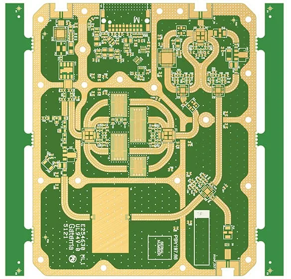
At 3 oz the etchant travels sideways through 105 µm of copper, so the minimum space opens to 0.20 mm and the trace section becomes a trapezoid.
Read article
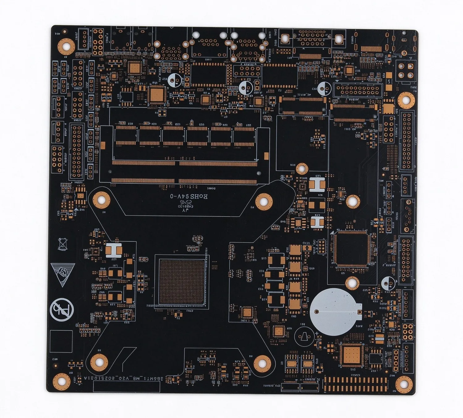
Six finishes on flatness, shelf life and cost, and the two questions that remove four of them immediately.
Read article
Send the thermal map and the die sizes. Quote in 24 hours, with the grade named rather than assumed. Every build runs to IPC Class 2 standard, Class 3 on request.