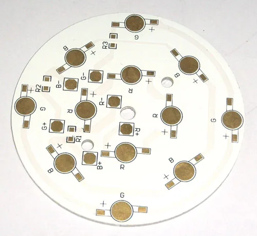
Metal Core LED Layout: Thermal Pad and Isolation Rules
The dielectric sets the thermal limit, not the aluminium: about 0.050 °C/W at 100 µm and 2 W/m·K under a 10 cm² source.
Read article

A heavy copper board is not a normal board with thicker foil. The etchant has to remove 105 µm of copper sideways to define a gap, the mask has to cover a step of the same height, and the plating has to throw copper into holes through a stack that is mostly metal. Each of those changes a design rule, not a process tolerance.
Subtractive etching works downward and sideways at once. In 35 µm foil the sideways travel is a small fraction of the trace width, so the finished trace is close to the artwork. In 105 µm foil the sideways travel is comparable to the feature size, and the artwork and the finished trace are different shapes.
Everything else follows from that. Minimum space grows because the etchant has to clear a deeper channel. Minimum width grows because a narrow trace loses proportionally more of itself. Tolerance grows because the two effects vary together, and the same percentage error is a larger absolute error on a heavier layer.
| Base weight | Thickness | Minimum trace | Minimum space |
|---|---|---|---|
| 1 oz, for comparison | 35 µm | 0.075 mm | 0.075 mm |
| 2 oz | 70 µm | 0.10 mm | 0.13 mm |
| 3 oz | 105 µm | 0.15 mm | 0.20 mm |
| 4 oz | 140 µm | 0.20 mm | 0.25 mm |
| 6 oz | 210 µm | 0.30 mm | 0.40 mm |
Windows are process capabilities for a given etching line and are confirmed against the shop before release. 4 and 6 oz are our standard heavy range; 12 oz is quoted on inquiry.
Space grows faster than width, and the reason is geometric. A narrow space is a deep channel that the etchant has to reach the bottom of, and in heavy copper that aspect ratio becomes the limit: a 0.15 mm space in 105 µm copper is a channel seven times deeper than it is wide, so fresh etchant reaches the bottom by diffusion rather than by flow. Width has a different limit — it is set by how much of the trace the sideways etch removes.
Where a design needs a fine feature on a heavy layer, the answer is usually to move the feature to a thin layer and connect through vias, or to use a pattern-plated process where copper is added rather than removed. Both cost process steps, and both beat a drawing that asks for 0.10 mm space in 3 oz copper.
Etch factor is the ratio of etched depth to lateral undercut. At an etch factor of 2, 105 µm of copper undercuts 52.5 µm per side, so a trace drawn at 0.20 mm at the bottom measures 0.305 mm at the top. That top width is what a drawing has to carry if the bottom is the requirement — which is why heavy copper drawings often quote two widths per trace. A designer who specifies one number is specifying the top and discovering the bottom in a cross-section.
Current flows through the cross-section, and the area of a trapezoid is the average of top and bottom times the thickness. For 0.305 mm top, 0.20 mm bottom and 105 µm, the average width is 0.2525 mm and the area is 0.0265 mm². Quoting the top width and multiplying by thickness overstates the copper by about 26% — a margin that disappears exactly when the design is tight.
Copper thickness, trace width, allowable temperature rise and the surrounding environment together determine the current, and none of them alone is a rating. A 3 oz trace at a 30 °C rise in still air carries roughly 10 A at 2 to 3 mm wide by the IPC-2152 method; the same trace in moving air, or at a 10 °C rise, carries less.
Resistance makes the point quickly. Three ounces is 0.162 mΩ per square, so a 10 mm run at 2 mm wide is five squares, or 0.81 mΩ. At 10 A that is 8.1 mV and 81 mW — small enough that the via stack, the connector and the solder joint become the terms that matter, not the trace.
A 6 oz layer at 210 µm is 0.081 mΩ per square, half the 3 oz figure. Doubling the copper roughly halves the resistive loss and adds process cost faster than it adds performance, which is why heavy copper stops paying before the current does — past a point the answer is a busbar rather than more foil, and that is a current-density question rather than a copper-weight one.
A via through a heavy stack has most of its length made of copper already, so plating has to build a wall in a hole whose ends are already thick. Aspect ratio — board thickness over drill diameter — is the usual limit: our standard is 12:1, and a heavy build sits at the tight end of that window because the wall has to be thrown through a stack that is mostly metal. Acceptance is read from the cross-section at 25 µm average and 20 µm at the thinnest point for Class 3 on boards of more than two layers.
Copper per barrel is a separate limit from copper on the surface. At a 0.3 mm drill and a 25 µm wall, a via carries about 0.8 A at a 10 °C rise, so a 20 A path needs an array rather than a hole. The surface can be 6 oz while the barrel is a thin cylinder, and it is the cylinder that fails first.
Where a via under a thermal pad has to be planar afterwards, it is filled and capped over plating to the Type VII construction, with coplanarity held around ±50 µm. On heavy copper the cap sits on a thicker step, so fill depth and planarity are specified together rather than inferred from the drill diameter.
Liquid photoimageable mask is 10 to 25 µm thick; the copper step at 3 oz is 105 µm. The film follows the step rather than levelling it, so it is thin on the shoulder and thick in the corner, and a dam between two heavy traces spans a channel four times its own thickness.
That makes dams a process decision rather than an artwork default: specify them by width and by the gap they span. Mask openings over heavy pads also want a larger expansion than on a thin layer, because the mask thins over the shoulder and a tight opening shows a ragged edge. Levelling adds to the step instead of filling it, so the final pad flatness depends on how the meniscus breaks on a thick edge.
Heavy copper on one face is a larger mass imbalance than the same weight on a thin board, so symmetry rules tighten rather than relax. The acceptance value for the finished board remains 0.75% under IPC-6012, and a 3 oz layer on one side of a 1.6 mm stack will test that limit — a build that plans for balance from the first stack-up draft is cheaper than one that discovers warp at press.
A heavy build adds etching time, plating time and often a second lamination. The reflow profile shifts as well: a board that is mostly copper has a thermal mass that takes longer to heat, so it sits at the top of the soak window rather than the bottom, and the assembly house needs that written down rather than inherited from the previous revision.
Around 0.15 mm trace and 0.20 mm space as a typical process window, against 0.075 mm on a 1 oz layer. The window belongs to the etching line, so it is confirmed against the shop before release rather than assumed from a table.
There is no bare width. At 3 oz, a 30 °C rise and still air the answer sits around 2 to 3 mm by the IPC-2152 method; change the rise or the airflow and the width moves with it. Copper area, not copper weight, is what the calculation returns.
The finished cross-section does — base foil plus plating. Panel plating and pattern plating add copper differently and are alternative routes rather than steps in series, so they are not summed. A coupon cross-section is what confirms the number.
It covers the step but does not planarise it, and a dam spanning a heavy copper channel is a thin film over a deep gap. Specify dams by width and by the gap they span, and expect the mask to be thinner on the shoulder than on flat laminate.
When the copper area needed exceeds what the process can etch, or when the cost of the extra weight passes the cost of a busbar. That is a current-density and assembly comparison rather than a copper-weight one, and it usually arrives earlier than designers expect.
The dielectric sets the thermal limit, not the aluminium: about 0.050 °C/W at 100 µm and 2 W/m·K under a 10 cm² source.
Read article
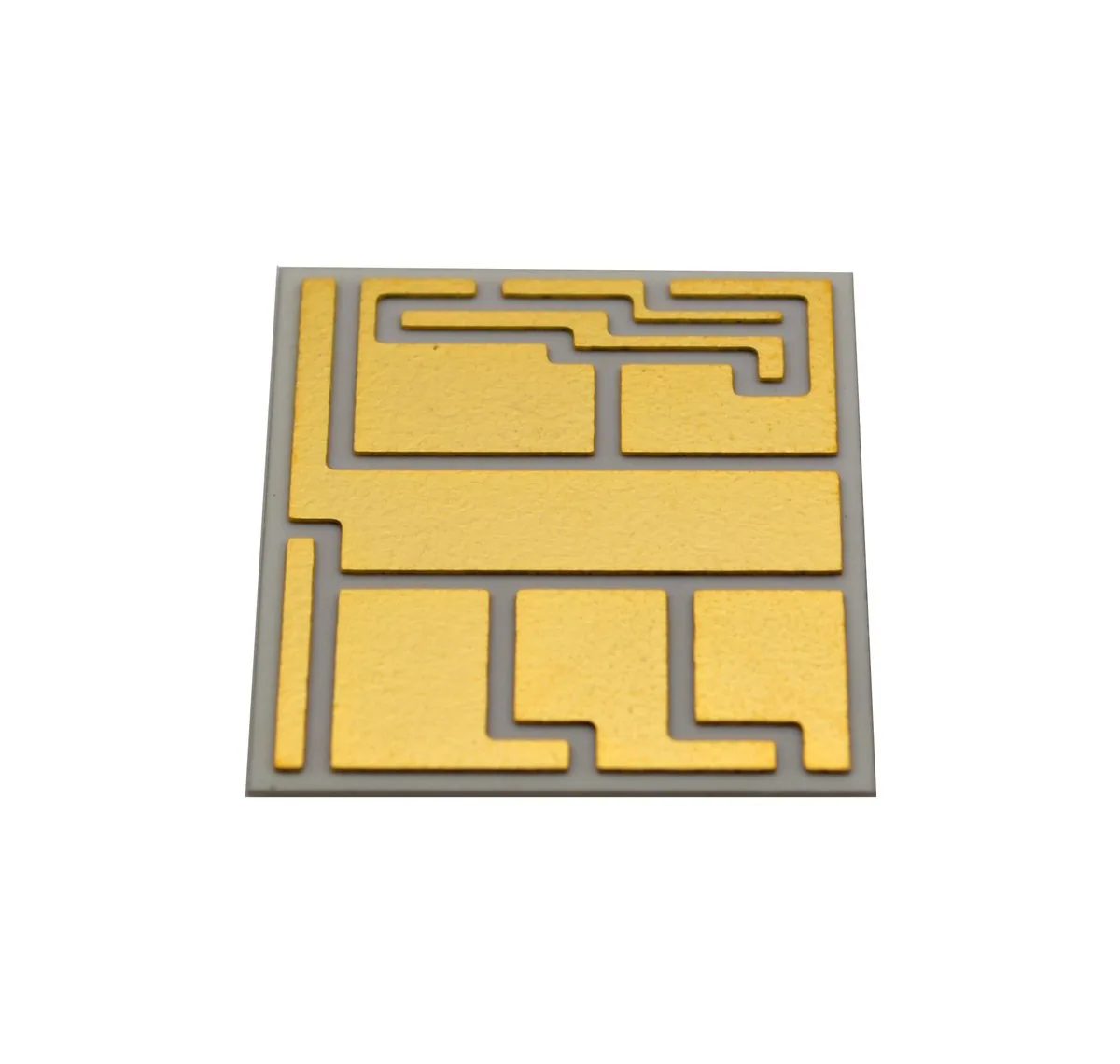
Alumina at 20–24 W/m·K and AlN at 170 against 0.2–0.3 for FR-4, plus the crossover arithmetic that decides which one ships.
Read article
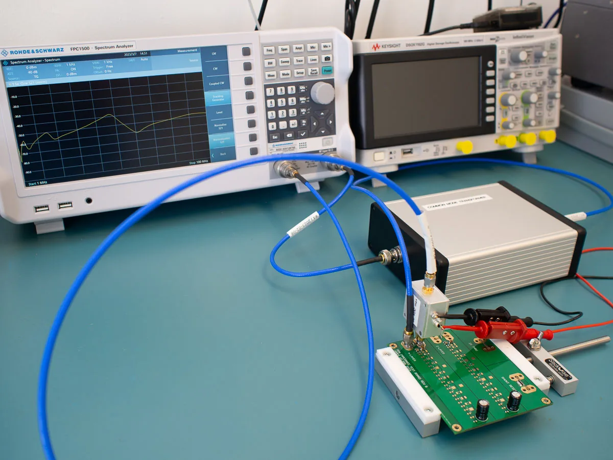
Four tolerances, four sensitivities, and why the root-sum-square lands at 7.1% while the worst case reaches 12%.
Read article
Send the stack-up with the copper weight per layer. Quote in 24 hours, with the etch window stated up front. Every build runs to IPC Class 2 standard, Class 3 on request.